|
| |
|
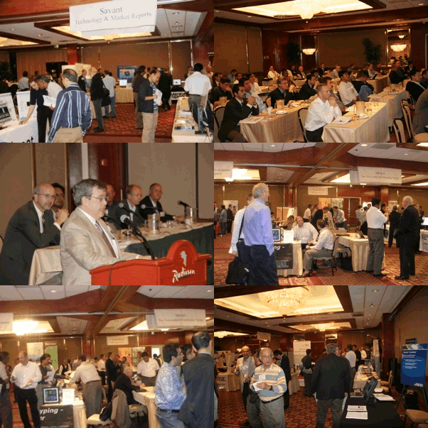
8th International System-on-Chip
(SoC)
Conference, Exhibit & Workshops
November 3 & 4, 2010
—
Hilton Irvine/Orange County Airport, Southern California
SoC Conference Presenters'
Bios & Abstracts
|
 |
|
If you
have any questions or need more information, please contact:
SoC@SavantCompany.com
or
949-851-1714
Thank
you!
|
|
|
|
|
|
|
|
|
|
Savant
Company Inc. |
 Farhad
Mafie, President and CEO of Savant Company Inc. Farhad
Mafie, President and CEO of Savant Company Inc.
"Welcome and Opening Remarks, Technology/Market Trends."
Seasoned technical executive
with extensive global experience in Semiconductor IC & IP businesses with
hands-on expertise in sales, marketing and engineering. Successful track
record in Start-up and Blue Chip companies.
Farhad is the former Vice
President of Marketing/Business Development and Technical Sales Engineering
teams at Toshiba America Electronic Components, Inc. He was responsible for
marketing the entire Toshiba standard ICs (RISC/CISC CPUs, Configurable
CPUs, DSPs, Bluetooth, Wireless ICs, RFID, MPEG-4, CCD/CMOS, Analog ICs,
Automotive ICs, etc.). He was also responsible for engineering development
for Toshiba's Embedded and Digital Consumer products & solutions based on
ASSP and SoC Models.
Farhad established Toshiba's on-line Tech-Support System as well as
Toshiba's on-line System Solution Selling methodologies for all Toshiba's
products in the North American markets. He also developed Toshiba's ASSP
Business Unit and Technical Sales Engineering Team as two brand new
organizations for the company.
Farhad has also worked at Lucent Technologies on marketing communications
ICs, Toshiba PC group on product definition for Toshiba's notebooks and
handheld products, Unisys on designing new processors and computer systems,
and MSI Data on designing data collection products. He has a MSEE and a BSEE
from California State University, Fullerton.
Farhad has a track record of success in large and start-up organizations,
building and leading strong sales, marketing and engineering teams, and in
improving traction and revenue with major international customers. He enjoys
developing business plan and go-to-market strategies for innovative and
disruptive technologies, deal making, developing strategic alliances and
partnerships.
He has more than 10 years of university-level teaching experience with
extensive experience in developing and conducting business and technology
seminars (e.g., RFID, CPUs, SoC/ASIC/FPGA Designs, Working Internationally,
Doing Business with China/Japan/India).
Farhad is the Editor-in-Chief, CRC Press, for SoC Design and Technologies
Book Series. Two New Books have been completed:
1) Low-Power NoC for High-Performance SoC Design
2) Design of Cost-Efficient Interconnect Processing Units
Farhad is also an author and a translator: Nader Naderpour (1929-2000)
Iranian Poet, Thinker, Patriot (Mellen Lives, V. 15.). May 2003. By
Farhad Mafie, The Edwin Mellen Press NY.
|
|
|
|
Conexant
Systems, Inc. |
 Dr.
Shireesh Verma, Imaging and PC Media Group, Conexant
Systems, Inc. Dr.
Shireesh Verma, Imaging and PC Media Group, Conexant
Systems, Inc.
Low Power Design Techniques -
Verification Challenges
Abstract: Power consumption
has become one of the critical factors for semiconductor products due to
ever increasing market demand for handheld consumer devices. It is a primary
design consideration for the majority of semiconductor designs now. It is
one of the key reasons behind the emergence of multi‐core designs as
increase in power consumption limits increases in clock speed at the rate we
have seen in the past. Voltage is a very effective tool for managing chip
power consumption. Power management techniques that leverage voltage are
being extensively used in power sensitive designs. These techniques include:
Power Gating (PG), Power Gating with Retention (RPG), Isolation, Multiple
Supply Voltages (MSV), Dynamic Voltage Scaling (DVS), Adaptive Voltage
Scaling (AVS), etc. The use of the power management techniques also implies
new challenges in verification of designs as new power states are created.
This talk addresses the verification challenges with these power management
techniques implemented on a chip. At physical level, dealing with multiple
power supplies and variable power supplies present us with many new
verification challenges. Can all of the power issues be addressed at the
frontend in the context of verification techniques? Or is it unrealistic to
even think that any true verification is possible without taking back‐end
into account? Why so much noise about power formats? Some of the largest
volume consumer electronic products are using these techniques and how are
the chips manufacturers getting them working in these products? Power‐aware
verification is a major concern for designs that are leveraging leading edge
power management techniques and this talk will explore these challenges
while providing useful recommendations.
Bio:
Shireesh Verma is
currently with Conexant Systems Inc. Prior to that he has held research and
development positions at Qualcomm Inc. and Marvell Semiconductor Inc.
He has been involved in extensive research on various aspects of
verification like, automatic generation and evaluation of functional and
syntactic coverage models, coverage feedback driven test generation,
behavioral error models, low power verification techniques, etc for the past
9 years. He obtained his PhD degree in Information and Computer
Science from the University of California Irvine. He has led several
in-house Design and Verification tool development efforts during his
industrial stints. He has published numerous conference papers, journal and
magazine articles and a book chapter. He has also delivered numerous invited
tutorials and has been invited at several panels in these areas. He
serves on the editorial board of Journal of Low Power Electronics (JOLPE).
He is also a member of the Accellera P1801 Low Power Working Group and the
IEEE Design Automation Standards Committee. He is a member of the Technical
Program Committees of "ACM/IEEE Design Automation and Test in Europe (DATE)
Conference", "IEEE International High Level design Validation and Test (HLDVT)
Workshop", and "International Symposium on Quality Electronic Design (ISQED)".
He is also a member of the organizing committee (Publicity chair) of the
HLDVT 2009.
|
|
|
|
Certicom Corp |
 Dan
O’Loughlin, Sr. Director of Product Management. Certicom Corp., A Subsidiary
of RIM Corporation. Dan
O’Loughlin, Sr. Director of Product Management. Certicom Corp., A Subsidiary
of RIM Corporation.
Designing In Hardware Root of Trust for Embedded Systems
Abstract: For both wireline and wireless applications, device authentication
and IP protection are looking to a hardware based root of trust to secure
digital transactions, digital media, as well as for securing software and
hardware intellectual property. While software is becoming more
sophisticated at defending against various forms of attack, the benefits of
each successive security patch are short lived. The benefits of a hardware
root of trust extend upward through each layer of a technology stack for any
given embedded system design. A strong hardware root of trust is capable of
extending a security standard or sub-standard's life expectancy and
providing a secure mechanism for managing sensitive digital assets.
Additionally, by providing a strong root of trust that is uniquely
provisioned to each device, the impact of any successful attack on a device
is restricted to only one device. Such an attack would also require a high
degree of sophistication and funding for each device, which would relegate
such attacks as economically impractical. There are two aspects to managing
an embedded system's digital assets: i) securely managing sensitive IP and
data throughout the manufacturing supply chain, and ii) securely managing
device authentications, setup/configuration, and/or post-production
feature/license provisioning throughout the distribution sales channel or
even directly to the end customer. In this regard, many system designers and
manufacturers are concerned that adding strong security will severely impact
the usability of their embedded system. By managing digital assets and
device authentication via a secure infrastructure that leverages a hardware
root of trust, the usability of any given embedded system may be minimally
impacted to maintain a high level of transparency to the end user for any
targeted electronic product vertical while enforcing new and evolving
licensing models.
Bio: Craig Rawlings started his career in 1985 as an engineer with Hewlett
Packard Electronic Design Division. From 1990 to 2000, Craig was with Actel
Corporation during the early start-up stages of the FPGA industry managing
the Pacific Rim and Silicon Valley strategic accounts businesses. In 2000,
Craig worked for Resilience as an Area VP of Sales, guiding sales and
business development for fault-tolerant Sun Solaris and Linux-Intel based
internet infrastructure appliances. In 2004, Craig joined Kilopass as the
Director of Marketing for embedded non-volatile memory IP prior to joining
Certicom as the Sr. Director of Product Management. Craig has earned a BSEE
and MBA from Brigham Young University and has published a number of articles
for technical publications such as Chip Design, Electronic Engineering
Times, and Nikkei Electronics. Craig also speaks fluent Japanese.
|
|
|
|
LSI Corporation |
 Robert
Madge, Director, Technology Marketing, LSI Corporation. Robert
Madge, Director, Technology Marketing, LSI Corporation.
A New Breed of ASIC for Networking Markets
Abstract: ASICs have been written-off as a viable silicon solution many
times in recent years due to the design complexity and implementation costs.
Some silicon suppliers have ventured into structured or platform ASICs to
help lower costs and speed time to market. The reality is ASICs and the need
for ASICs never went away. Significant hardware differentiation can be
achieved by system providers using ASICs that cannot be realized using
standard products or software. What is required instead is a viable business
model for Intellectual Property (IP) development and ASIC design
implementation that enables a win-win for both customers and suppliers in a
fabless model. The new LSI model for ASIC design and IP implementation feeds
off a foundation library of IP, re-used among ASIC and standard products. A
single design flow integrates this IP into standard product, an ASIC, or
various options in-between the two. IP can be designed with foundry
portability in mind, if required; otherwise the IP and design flow is
targeted to a single foundry technology. The new ASIC model’s success rests
on two main factors. One, the IP and design technology is targeted toward
the networking market (Examples include power management, multi-core
processing, SerDes protocols, and embedded DRAM.) Second, the high amount of
IP re-use allows for a successful and scalable business model, including the
ability to continue to invest in leading edge technologies.
Bio: Robert Madge is a director of Technology Marketing at LSI responsible
for strategic marketing of LSI’s ASIC products and technology roadmap. Madge
was responsible for LSI’s 65nm and 40nm technology introduction and is
currently driving the LSI’s 32/28nm Technology Planning. Madge joined LSI in
1989, and has held various product engineering positions in the United
States, Europe and Hong Kong. While in Hong Kong, he set up the Pan-Asian
Test and Product Engineering Operations. Madge has written over 20 papers
and holds twelve patents in the areas of Test, Yield and Design for
Manufacturing and is a regular industry presenter and panelist. He was
awarded best paper awards at International Test Conference (ITC) 2000 and
VLSI Test Symposium (VTS) 2003 and was the Invited Plenary Speaker at ITC in
2004. Madge graduated from Sheffield University in England.
|
|
|
|
X-Fab
Semiconductor Foundries |
 Mark
A. Miller, V.P. Business Development, X-Fab Semiconductor Foundries. Mark
A. Miller, V.P. Business Development, X-Fab Semiconductor Foundries.
Exploring opportunities for the integration of silicon and biotechnology.
Abstract: The semiconductor
industry has transitioned through numerous boom and bust cycles over the
past four decades. These have been driven, in large part, by underlying
high-growth market developments, including the personal computer, mobile
communications, the internet, high definition digital multimedia, and mobile
social networking. We now stand on the frontier of a new developing market
opportunity, silicon-based biotech that shows the promise to act as the
driving force in the evolution for both biotech and semiconductor technology
providers. The scalability, substantial cost reduction, and opportunity for
massive parallelism afforded by semiconductor technology will provide the
next development platform for the biotech industry. This paper will explore
some of the technology foundations underlying this topic as well as
highlighting example applications already under development, their technical
and economic benefits.
Bio: Mark Miller is the vice president of business development for XFab
Semiconductor Foundries. Prior to joining XFab, he was vice president of
marketing and business development for DFM products at Cadence Design
Systems, a leading provider of Electronics Design Automation (EDA) software
and services. He also held similar positions at Tera Systems, a provider of
silicon virtual prototyping solutions, Synchronicity, a leader in design
reuse, collaboration and management solutions for electronic product
development, and Mentor Graphics, as director of its IC Technology Center.
An electrical engineering graduate of Rensselaer Polytechnic Institute, he
has over twenty five years of sales, marketing, product development and
design experience in the semiconductor and EDA industries.
|
|
|
|
Morning Break |
Morning Break
|
|
|
|
IBM
Keynote
|
 Dr.
Juan-Antonio Carballo, WW Manager, IBM Microelectronics Services,
Semiconductor Partner, IBM VC Group. Dr.
Juan-Antonio Carballo, WW Manager, IBM Microelectronics Services,
Semiconductor Partner, IBM VC Group.
Keynote
Dr.
Juan-Antonio Carballo is IBM Corporation's Venture Capital Executive for
Semiconductors and Hardware Systems, responsible for creating and managing
strategic projects with top-tier Venture Capital firms and their portfolio
companies. Prior to this role, Juan-Antonio was leading research in adaptive
communications chips at IBM Research. He won an IBM Research Division award
for his work in this area. He filed 23 patents and has over 20 publications
in low-power design, communications systems, design economics, and
electronic design management. He is the Chair of the International
Technology Roadmap for Semiconductors (ITRS) Design and System Drivers
Chapters, the Chair Elect of IEEE's DATC Committee, and VSIA's R&D Chair in
2004-5. He has been on the committee of six symposiums and conferences, and
was the General Chair for Electronic Design Processes
2004 in Monterey, CA. His prior work experience includes stays at Digital
Equipment (currently HP) and LSI Logic. Juan-Antonio holds a Ph.D. in
Electrical Engineering from the University of Michigan, an M.B.A. from the
College des Ingenieurs (Paris),and a M.Sc. in Telecommunications Engineering
from the Universidad Politecnica de Madrid.
|
|
|
|
Panel |
"Exploring Opportunities for the Integration of Silicon and Biotechnology"
|
|
|
|
X-Fab
Semiconductor Foundries
USC
UCSD
UCI
UCLA
Canadian Consulate General |
 Mark
A. Miller, V.P. Business Development, X-Fab Semiconductor Foundries Mark
A. Miller, V.P. Business Development, X-Fab Semiconductor Foundries
Moderator
Mark Miller is the vice president of business development for XFab
Semiconductor Foundries. Prior to joining XFab, he was vice president of
marketing and business development for DFM products at Cadence Design
Systems, a leading provider of Electronics Design Automation (EDA) software
and services. He also held similar positions at Tera Systems, a provider of
silicon virtual prototyping solutions, Synchronicity, a leader in design
reuse, collaboration and management solutions for electronic product
development, and Mentor Graphics, as director of its IC Technology Center.
An electrical engineering graduate of Rensselaer Polytechnic Institute, he
has over twenty five years of sales, marketing, product development and
design experience in the semiconductor and EDA industries.
Panelists:
1. Professor Alice C. Parker, The BioRC Biomimetic Real-Time Cortex Project,
Department of Electrical Engineering, USC.
2. Professor Yu-Hwa Lo, Department of Electrical and Computer Engineering,
Specializes in Photonic Integrated Circuits, UCSD.
3. Dr. Jim Brody, Associate Professor Biomedical Engineering, UCI.
4. Chi On Chui, Ph.D., Assistant Professor of Electrical Engineering, UCLA.
5. Mohammad E. Kondri, MPH, MIS/MBA, International Business Development
Officer, Trade Commissioner, Life Sciences & Medical Technologies, Canadian
Consulate General.
6. TBA
|
|
|
|
USC |
 Alice
C. Parker, Professor of Electrical Engineering, University of Southern
California. Alice
C. Parker, Professor of Electrical Engineering, University of Southern
California.
Panelist
Alice C. Parker is a Professor
of Electrical Engineering at the University of Southern California and is a
former Division Director for Computer Engineering, a former Dean of Graduate
Studies, and a former Vice Provost for Research at USC. She was elected
President of the Academic Senate in 1993. She was previously on the faculty
at Carnegie Mellon. Dr. Parker received the B.S.E.E. and Ph.D degrees from
North Carolina State University and an M.S.E.E. from Stanford University.
She was elected a Fellow of the IEEE for her contributions to design
automation in the areas of high-level synthesis, hardware description
languages and design representation. She also received an NSF Faculty Award
for Women Scientists and Engineers, an NSF Fellowship, and an teaching award
from the Viterbi school. She received the ASEE Sharon Keilor Award in 2009,
and an award from South Central Scholars for her community outreach in 2008.
BioRC, Biomimetic Real-time Cortex, is Dr. Parker's current research. She is
designing CMOS and carbon nanotube neural nanocircuits, and investigating
the timetable for a possible synthetic cortex based on statistical
predictions.
Dr. Parker has performed high-level synthesis research since 1975, and was
one of the earliest such researchers. She is also known for her research in
design data structures, CAD databases, and hardware descriptive languages.
In the early 1990's Dr. Parker and her group used a combination of their
software along with a commercial silicon compiler to produce an integrated
circuit layout from the functional specification in under 48 hours. Her
research in the past decade focused on system-level synthesis and
partitioning, including the automatic design of multimedia network hardware
and data management.
|
|
|
|
UCSD |
 Dr.
Yu-Hwa Lo, Electrical and Computer Engineering, UCSD. Dr.
Yu-Hwa Lo, Electrical and Computer Engineering, UCSD.
Panelist
Dr. Yu-Hwa
Lo received his PhD in electrical engineering from UC Berkeley in 1987. He
was a Member of Technical Staff at Bellcore (now Telcordia) from 1988 to
1990. In 1991, he joined the faculty of School of Electrical Engineering,
Cornell University as an Assistant Professor and then became an Associated
Professor. He became a professor of ECE Department of UCSD since 1999. Dr.
Lo maintained a broad interest in several research areas, including
optoelectronic materials and processing, optoelectronic devices,
semiconductor lasers, optical MEMS, an more recently microfluidics,
biophotonics, nanodevices, and biomedical systems-on-chips. His research is
multidisciplinary and involves close collaborations with other academic and
industrial groups. Current Research: Single photon detection for optical
communication, sensing, and imaging. Microfluidic-photonic-acoustic
integrated circuits for biomedical systems-on-chips. Bio-inspired optic
devices and systems. Investigation of fundamental biomolecular
interactions/properties using nanophotonic approaches.
|
|
|
|
UCI |
 Dr.
Jim Brody, Associate Professor, Biomedical Engineering, UCI. Dr.
Jim Brody, Associate Professor, Biomedical Engineering, UCI.
Panelist
Dr.
Jim
Brody has published over 40 refereed journal and conference papers. He is
also a named inventor on over a dozen patents. His current research
interests are in applications of technology to experimental genetics.
Earlier in his career, he participated in founding Micronics, a developer of
point-of-care diagnostic tests based on a micro-fluidic platform. Currently,
he is an associate professor of Biomedical Engineering at the University of
California, Irvine.
He
graduated with degrees in Physics from MIT (BS, 1989) and Princeton (PhD,
1994). Before joining UC Irvine, he was a postdoc at the University of
Washington in Bioengineering (1994-1998) and at Caltech in Applied Physics
and Biology (1998-2000).
|
|
|
|
UCLA |
 Chi
On Chui, Ph.D., Assistant Professor of Electrical Engineering, UCLA. Chi
On Chui, Ph.D., Assistant Professor of Electrical Engineering, UCLA.
Panelist
Chi On Chui
received the B.Eng. degree in Electronic Engineering (with highest honors)
from the Hong Kong University of Science and Technology (HKUST) in 1999, and
the M.S. and Ph.D. degrees in Electrical Engineering from Stanford
University in 2001 and 2004, respectively. He joined the Intel Corporation
as a Senior Device Engineer in 2004 to research and evaluate post-silicon
transistor technologies for high performance logic applications. During his
tenure with Intel, he served as a Researcher-in-Residence at the University
of California, Berkeley and at Stanford University. From 2005-2006, he was
also appointed Consulting Assistant Professor of Electrical Engineering at
Stanford University. In January 2007, he joined the faculty of the
University of California, Los Angeles (UCLA) as an Assistant Professor of
Electrical Engineering. Since 2009, he has been an elected Member of the
UCLA’s California NanoSystems Institute (CNSI).
Dr. Chui is an early advocate
of the use of high mobility semiconductor in MOSFETs and seminally
demonstrated the incorporation of nanoscale high-permittivity gate
dielectrics for germanium MOS device applications. His research group at
UCLA currently focuses on developing top-down and bottom-up nanotechnology
for nanoarchitectonics, biomedical electronics, and terahertz electronics.
Dr. Chui has received several
awards including HKUST’s Academic Achievement Award (AAA) in 1999, the Intel
Foundation Ph.D. Fellowship in 2003, the Microsoft Academic Research Grant
in 2003, the Okawa Foundation Award in 2007, and very recently the IEEE
Electron Devices Society Early Career Award in 2009. In addition, his works
have won the best paper awards at the IEEE 60th Device Research Conference (DRC)
in 2002 and the 13th Workshop on Dielectrics in Microelectronics (WoDiM) in
2004. He has delivered one keynote speech and numerous invited talks. He is
a named inventor on three issued patents, and few other pending patents in
semiconductor device technology. He has authored or co-authored more
than 75 peer-reviewed archival journal and conference papers (including two
review papers and 21 invited papers) and four book chapters.
|
|
|
|
Canadian Consulate General |
 Mohammad
E. Kondri, MPH, MBA, International Business Development Officer, Mohammad
E. Kondri, MPH, MBA, International Business Development Officer,
Trade Commissioner, Life Sciences & Medical Technologies, Canadian Consulate
General.
Panelist
Mohammad E. Kondri is a Trade
Commissioner, International Business Development, Life Sciences and Medical
Technology Officer at the Canadian Consulate General in Los Angeles. With
Over 25 years of drug discovery, pharmaceutical development, and technology
management experience working at non-profit cancer research institution,
pharmaceutical industry and government. Prior to joining the Canadian
Consulate, he was Associate Director of Operations at Covance Bioanalytical
and Immunology Laboratory Services Division and worked as a Senior Research
Scientist and Corporate Technology Transfer liaison at Bristol-Myers Squibb
Pharmaceutical Research Institute and Fred Hutchinson Cancer Research Center
in Seattle. He has authored and co authored several publications in the
areas of gene expression, DNA manipulations, cancer and immunology drug
development, contributed to commercialization of five drug candidates, and
holds several patents with potential drug development applications. He has
a MPH in Molecular Microbiology and Public Health from Washington State
University and MIS/MBA in Technology Management from Steven’s Institute of
Technology.
|
|
|
|
Lunch |
Lunch @ Pavilion . . .
|
|
|
|
Panel |
“Improving Design Productivity and IP Quality through the Effective Use of
Standards for Complex Multicore SoCs"
|
|
|
|
IBM
Virage Logic
Accellera
Tabula Inc.
SPIRIT Consortium
IPextreme
GDA Technologies
Rapid Bridge |
 Dr.
Juan-Antonio Carballo, WW Manager, IBM Microelectronics Services,
Semiconductor Partner, IBM VC Group. Dr.
Juan-Antonio Carballo, WW Manager, IBM Microelectronics Services,
Semiconductor Partner, IBM VC Group.
Moderator
Dr.
Juan-Antonio Carballo is IBM Corporation's Venture Capital Executive for
Semiconductors and Hardware Systems, responsible for creating and managing
strategic projects with top-tier Venture Capital firms and their portfolio
companies. Prior to this role, Juan-Antonio was leading research in adaptive
communications chips at IBM Research. He won an IBM Research Division award
for his work in this area. He filed 23 patents and has over 20 publications
in low-power design, communications systems, design economics, and
electronic design management. He is the Chair of the International
Technology Roadmap for Semiconductors (ITRS) Design and System Drivers
Chapters, the Chair Elect of IEEE's DATC Committee, and VSIA's R&D Chair in
2004-5. He has been on the committee of six symposiums and conferences, and
was the General Chair for Electronic Design Processes
2004 in Monterey, CA. His prior work experience includes stays at Digital
Equipment (currently HP) and LSI Logic. Juan-Antonio holds a Ph.D. in
Electrical Engineering from the University of Michigan, an M.B.A. from the
College des Ingenieurs (Paris),and a M.Sc. in Telecommunications Engineering
from the Universidad Politecnica de Madrid.
Panelists:
1. Dr. Karen Pieper is Director of
Synthesis at Tabula Inc. & Technical Chair for Accellera.
2. Dr. Gary Delp, VP and Technical
Director of the SPIRIT Consortium and Principal of the consulting firm
Silver Loon Systems.
3. Warren Savage, President & CEO,
IPextreme.
4. Michael Brunolli, Co-Founder and CTO,
Rapid Bridge.
5. Ken Brock, Product Line Director.
Virage Logic
6. Ravi Thummarukudy, VP& GM, IC
Solutions Business Unit and Co-Founder, GDA Technologies.
|
|
|
|
IPextreme |
 Warren
Savage, President & CEO, IPextreme. Warren
Savage, President & CEO, IPextreme.
Panelist
Warren
Savage • President & CEO, prior to founding IPextreme, Mr. Savage created
and ran the Star IP Program at Synopsys, where he provided an IP brokering
function for major semiconductor companies. Prior to that, Mr. Savage was
head of the Synopsys DesignWare engineering organization, where he
introduced many design practices and quality measures, which eventually
became part of the Reuse Methodology Manual, a seminal book on Intellectual
Property design. From 1982-1995 he worked for Tandem Computers, and there
developed an interest in advanced design methodologies around high
reliability design. Mr. Savage began his career at Fairchild Semiconductor
developing semiconductor test equipment. Mr. Savage is a well-known and
published authority in the field of semiconductor intellectual property. Mr.
Savage has a BS in Computer Engineering from Santa Clara University and an
MBA from Pepperdine University.
|
|
|
|
Virage Logic |
 Kenneth
Brock, Director of Physical IP Marketing, Virage Logic. Kenneth
Brock, Director of Physical IP Marketing, Virage Logic.
Panelist
As Virage
Logic’s Director of Physical IP Marketing, Mr. Brock is responsible for
driving the company’s logic product line to meet the industry’s requirements
for advanced node IP solutions that deliver optimal performance, power, area
and yield. Mr. Brock has more than twenty-five years experience in the IP
and EDA industries serving in marketing, management, professional services,
and product development roles at Simucad, Virtual Silicon, Collett
International, Compass Design Automation, Mentor Graphics, and Silicon
Compilers. Mr. Brock holds a BSEE and MBA from Fairleigh Dickinson
University.
|
|
|
|
Accellera
Tabula
Inc. |
 Dr.
Karen Pieper is Director of Synthesis at Tabula Inc. & Technical Chair for
Accellera. Dr.
Karen Pieper is Director of Synthesis at Tabula Inc. & Technical Chair for
Accellera.
Panelist
Karen
Pieper is Director of Synthesis at Tabula Inc., and was formerly Director of
Synthesis at Synopsys. She is currently serving as the Chair of the IEEE
1800 SystemVerilog Working Group and as the Technical Chair for Accellera.
She has also served as Accellera's TC Co-Chair and Co-Chair of Accellera's
SystemVerilog-Basic Committee. She has been an active participant in Verilog
standardization since 1995. In 2005, she was a co-recipient of Accellera's
Technical Excellence Award. She has a Bachelors degree in Computer Science
from Rice University and a PhD. in Computer Science from Stanford
University.
|
|
|
|
The SPIRIT
Consortium |
 Dr.
Gary Delp, VP and Technical Director of the SPIRIT Consortium and Principal
of the consulting firm Silver Loon Systems. Dr.
Gary Delp, VP and Technical Director of the SPIRIT Consortium and Principal
of the consulting firm Silver Loon Systems.
Panelist
Gary Delp
is VP and Technical Director of the SPIRIT Consortium and Principal of the
consulting firm Silver Loon Systems. As an invited member of the Si2 Low
Power Coalition Format working group (CPF), vice-chair of the IEEE P1801 (UPF)
and Secretary of P1685 (IP-XACT) he is in a unique position to provide
insight into interoperability needs and potentials. Gary spends his time
working on design and IP reuse, including inside of a design, across
designs, and across the economic eco-system. Some of this reuse is in the
form of bundles and IP functions, while some is in the form of formats,
methodologies, and exploratory work. Standards Setting bodies, Industry
Alliances and University research programs support this work of technology
transfer. He enjoys working collaboratively, which is demonstrated by the
fact that the bulk of his 50 patents are jointly held with others. Gary
holds a PhD in Electrical Engineering and an MFA in theatre. He once managed
to integrate both when he led a team in building 2 full sized mountains for
an outdoor historical drama.
|
|
|
|
Rapid Bridge |
 Michael
Brunolli, Chief Technology Officer, Rapid Bridge. Michael
Brunolli, Chief Technology Officer, Rapid Bridge.
Panelist
Michael Brunolli has over 25
years of digital and analog integrated circuit (IC) design experience and
holds 18 patents. As a Division Fellow with Brooktree Corporation, Mr.
Brunolli pioneered the development of high speed RAMDACs. For his BT458, he
was given the "NCGA 1991 Award for Technical Excellence." Later with
Rockwell Semiconductor Systems, Mr. Brunolli contributed various analog
cores for video and modem products. As a result, in 1996 he was honored as
Rockwell's "Engineer of the Year." In 1997, he co-founded NurLogic Design
Inc., where he developed PLLs, high speed IOs, A/D and optical communication
technology. For its 48 channel optical design, NurLogic won USCD CONNECT's
Most Innovative New Product of the year Award in 2001. Nurlogic was acquired
by Artisan Components in February of 2003. Mr. Brunolli earned a B.S. in
Electrical and Computer Engineering from the University of California,
Davis.
|
|
|
|
GDA |
 Ravi
Thummarukudy, VP& GM, IC Solutions Business Unit and Co-Founder, GDA. Ravi
Thummarukudy, VP& GM, IC Solutions Business Unit and Co-Founder, GDA.
Panelist
Ravi Thummarukudy, Vice
President and General Manager of the IC Solutions Division, has over 18
years of experience in the semiconductor/EDA industry. Before co-founding
GDA, he held Global Business and Technology Management positions at Cadence
Design Systems as well as System Analyst position at Tata Consultancy
Services and a Senior Scientist position at the Indian Space Research
Organization (ISRO). He has extensive experience in defining and perceiving
customers' design requirements and providing creative solutions for
semiconductor and system OEMs. He gained insight into the Global IT service
business while at TCS. At Cadence, he learned how to manage major customers
and keep them for the long term. He developed a knack for recognizing the
need for services to enable customers to absorb newer technologies as well
as the need for additional capacity for electronic design services. Excited
by this vision of becoming a value-added IP and service business around the
globe, he ventured into GDA with AGK and Gopa. His strong association with
NEC and Cadence helped establish infrastructure and credibility for IC
services in the early days at GDA. Also at GDA, he found additional value
came from specialization, via building several intellectual property blocks
ahead of the market needs. Contributing to GDA's global viewpoint,
Thummarukudy has several years of experience in developing partnerships with
silicon vendors in the USA and Japan. His background is, in fact,
tremendously varied. He has previously been Chair of the Hyper Transport
Consortium Business Task force. He has taught Deep Sub Micron Design classes
at the University of Santa Cruz extension. He holds an MSEE from IIT Madras
and an MBA from Santa Clara University. Ravi has contributed several
articles on IC design to ISD Magazine, Chip Design Magazine and Electronic
Design . He enjoys gardening, painting, and fishing in his leisure
time.
|
|
|
|
Freescale
Keynote
|
 Ken Hansen, Sr.
Fellow, Vice President and Chief Technology Officer (CTO),
Freescale. Ken Hansen, Sr.
Fellow, Vice President and Chief Technology Officer (CTO),
Freescale.
Keynote
Ken Hansen is sr. fellow, vice
president and chief technology officer with Freescale Semiconductor. Prior
to becoming CTO, Ken was vice president in the chief development office
where he focused on improving design efficiency and reducing product cost
across all the Freescale businesses. Previously, he held several senior
technology and management positions at Freescale and Motorola leading
research and development teams.
He received his BSEE and MSEE from the University of Illinois, is a Senior
Member of the IEEE, and holds 12 U.S. patents. Ken is an industry veteran,
with 33 years of analog and digital design experience in bipolar, CMOS, and
BiCMOS technologies primarily in the area of wireless communications.
|
|
|
|
Afternoon Break |
Afternoon Break
|
|
|
|
Target Compiler Technologies |
 Steve
Cox & Gert Goossens, Target Compiler Technologies - Leuven, Belgium and
Boulder, CO USA. Steve
Cox & Gert Goossens, Target Compiler Technologies - Leuven, Belgium and
Boulder, CO USA.
ASIPs: Programmable Accelerators for Multicore SoCs – A High-Throughput JPEG
Encoder Case Study
Abstract: Offloading computationally intense functionality from processors
to hardware accelerators in order to meet performance and power requirements
is a common design technique. ASIPs deliver the same benefits, but without
sacrificing programmability. This presentation will focus on the key
enabling technologies that make ASIP development a viable (and valuable)
methodology for any SoC design team. A case study is presented for a
high-throughput JPEG encoder developed for still camera and scanning
applications. The natural decomposition of the JPEG algorithm across two
distinct programmable cores, and the details of each core are described.
Details such as performance, silicon efficiency, and design time are
described.
Bio: Steve Cox joined Target Compiler Technologies in 2006 and leads
Target’s North American activities. Steve has a long history of innovation
in the design and verification of processors and SoCs, including work at
companies such as Accelchip, Apple, Ball Aerospace, Cadence, Cisco,
Conexant, Intel, Motorola/Freescale, Nortel, and Solbourne Computer. Steve
holds patents in the area of transaction-based verification of SoCs and is
an alumnus of the University of Colorado. Steve currently resides in
Boulder.
Bio: Dr. Gert Goossens is the CEO and a co-founder of Target Compiler
Technologies, the leading provider of retargetable tools for the design of
application-specific processors. Before founding Target in 1996, Gert was
affiliated with the IMEC research centre, where he headed research groups on
high-level synthesis and software compilation. Gert holds several patents in
the area of processor modeling and design, and has authored or co-authored
around 40 papers in electronic design automation, several of which received
best-paper awards. Gert received MS and Ph.D degrees in electrical
engineering from K.U. Leuven.
|
|
|
|
Triad Semiconductor, Inc.
|
 Jim
Kemerling, CTO, Triad Semiconductor, Inc. Jim
Kemerling, CTO, Triad Semiconductor, Inc.
Via-Configurable, Mixed-Signal Embedded ASICs Using the ARM Cortex-M0
Microcontroller
Abstract: This presentation will introduce ARM powered mixed-signal
via-configurable array (VCA) ASIC technology as a means for resolving many
issues confronting analog/mixed-signal designers—HW/SW development time and
tooling cost. VCA mixed-signal ASICs are programmed with a single via layer.
Combining mixed-signal VCA technology with the 32 bit ARM Cortex-M0
microcontroller provides a level of performance, configurability, and
integration ideal for some embedded SoC applications. A new VCA architecture
with an embedded Cortex-M0 will be discussed in detail along with a
mixed-signal design example.
Bio: Jim Kemerling is the Chief Technical Officer of Triad Semiconductor,
Inc. At Triad he is responsible for VCA technology development and
implementation. His background includes over 25 years of experience with
mixed-signal integrated circuit design and system-level development. Jim
holds two patents and has published numerous papers. He received his BSEE
from South Dakota State University and his MSEE from the University of
Nevada.
|
|
|
|
ARM |
 Dr.
Mrinmoy Ghosh, Research and Development, ARM. Dr.
Mrinmoy Ghosh, Research and Development, ARM.
System-Level Performance Analysis of ARM based SoCs.
Abstract: As mobile applications and devices become ubiquitous, consumer
demands for performance, power efficiency, and connectivity are increasing.
The software framework on Mobile Internet Devices and Smartphones is a
complex interaction of real-time tasks, non-real-time applications, and
operating system management routines. Traditional simulation approaches are
poorly suited to modeling the overall performance characteristics of such
systems. Additionally, many traditional benchmark suites used in academia
and industry for microprocessor benchmarking and design have been found to
be unrepresentative of mobile workloads.
In this talk, we present multiple frameworks utilized for accurately
modeling system level performance of embedded systems. We also provide an
in-depth workload characterization and memory-level analysis of internet and
media-centric applications. On these realistic applications, we describe the
performance advantages of a two and four byte variable length instruction
set, Thumb2, over a four byte fixed length instruction set, ARM.
Bio: Mrinmoy Ghosh is a Senior Design Engineer in the Research and
Development group at ARM. He has worked at ARM for a year on system level
analysis and memory hierarchy optimizations. He received his Ph.D. from
Georgia Institute of Technology, and his M.S. and B. Tech from Indian
Institute of Technology, Kharagpur.
|
|
|
|
PixSil Technology Corporation |
 John
Johl, Advanced Architectures LLC, PixSil Technology Corporation. John
Johl, Advanced Architectures LLC, PixSil Technology Corporation.
IP for Video Compression Decoder (H.264)
Abstract: Advanced Architectures and PixSil Technology have developed
several hardware IP blocks for the H.264 video compression standard. These
blocks are highly modular and designed to be embedded within a
System-on-chip (SOC). The A2P processor manages most of the high-level
functions as well as setting the parameters for control of the data stream.
Many of the different profiles and levels of the H.264 standard are
configured by setting the desired parameters of each block for the desired
system. This concept is applied to the Variable-Length Decoder,
Context-based Adaptive Variable Length Decoder, Context-based Adaptive
Binary Arithmetic Decoder, and Inverse Integer Transform Block of the H.264
algorithm stream. Motion Compensation and De-blocking filters are also
handled by the A2P processor.
Bio: Dr. Johl is currently Senior Design Engineer at PixSil Technology,
where he is developing architectures and implementations for H.264
algorithms. He has extensive experience in ASIC architecture design,
specifically in the area of signal and image processing. Previously, he was
working on MPEG video compression at Mediaworks and sensor pre-processing
applications at Newport Imaging. In addition, as Technical Manager at
Intrinsix, he led several design and verification SOC projects including a
Memory Translator ASIC and SDRAM Buffer for DVD chip. John Johl has
accumulated over 25 years experience in both the defense (Hughes, TRW and
McDonnell Douglas) and commercial industries related to signal and image
processing. Prior to his work in aerospace, he taught digital logic and
microprocessor courses at California Statue University, Northridge, as
Assistant Professor in Electrical and Computer Engineering and performed
research in parallel algorithms such as the VLSI Reed-Solomon encoder and
decoder while at the Jet Propulsion Laboratory. Dr. Johl obtained his PhD
from the University of Southern California, his MSEE from Carnegie-Mellon
University, and his BSEE from M.I.T.
|
|
|
|
MCST
Russia |
 Sergey
A. Cherepanov, Technical Lead, MCST, Russia. Sergey
A. Cherepanov, Technical Lead, MCST, Russia.
MCST-4R – SPARC-V9 compatible scalable SoC design.
Abstract: MCST-R is a superscalar in-order core that implements 64-bit
SPARC-V9 instruction set. The key core features are: 2-wide superscalar
design, write-back non-blocking L1 data cache, floating point unit with
fused multiply-add support and short pipeline. 7-stage pipeline allows to
achieve 1GHz frequency using TSMC 90nm process. MCST-R core is designed for
a wide variety of applications from embedded systems to small servers. Based
on MCSR-R core multicore MCST-4R SoC has been implemented. It has 4 cores
integrated with shared L2 cache, DDR2 memory controller and IO host bridge.
Also, NUMA glue logic is integrated on the die that allows to build 16-core
system on the base of MCST proprietary protocol. Optimizing and
automatically parallelizing compiler is used to help better utilization of
system computational resources.
Bio: Sergey Cherepanov received M.S.E.E. from Moscow Institute of Physics
and Technology in 2002 and joined MCST in 2000. He has been involved in
memory subsystem design, FPGA prototyping and post-silicon validation for
several MCST microprocessors. He is currently working on the next generation
MCST-R microprocessor as technical lead of memory subsystem design.
|
|
|
|
|
|
|
|
|
Conference Day Two
Thursday, November 5, 2009
|
Conference Day Two
Thursday, November 5, 2009
|
|
|
|
|
|
|
|
|
Savant
Company Inc. |
 Farhad
Mafie, President and CEO of Savant Company Inc. Farhad
Mafie, President and CEO of Savant Company Inc.
Welcome and Opening Remarks, Conference Update.
Seasoned technical executive
with extensive global experience in Semiconductor IC & IP businesses with
hands-on expertise in sales, marketing and engineering. Successful track
record in Start-up and Blue Chip companies.
Farhad is the former Vice
President of Marketing/Business Development and Technical Sales Engineering
teams at Toshiba America Electronic Components, Inc. He was responsible for
marketing the entire Toshiba standard ICs (RISC/CISC CPUs, Configurable
CPUs, DSPs, Bluetooth, Wireless ICs, RFID, MPEG-4, CCD/CMOS, Analog ICs,
Automotive ICs, etc.). He was also responsible for engineering development
for Toshiba's Embedded and Digital Consumer products & solutions based on
ASSP and SoC Models.
Farhad established Toshiba's on-line Tech-Support System as well as
Toshiba's on-line System Solution Selling methodologies for all Toshiba's
products in the North American markets. He also developed Toshiba's ASSP
Business Unit and Technical Sales Engineering Team as two brand new
organizations for the company.
Farhad has also worked at Lucent Technologies on marketing communications
ICs, Toshiba PC group on product definition for Toshiba's notebooks and
handheld products, Unisys on designing new processors and computer systems,
and MSI Data on designing data collection products. He has a MSEE and a BSEE
from California State University, Fullerton.
Farhad has a track record of success in large and start-up organizations,
building and leading strong sales, marketing and engineering teams, and in
improving traction and revenue with major international customers. He enjoys
developing business plan and go-to-market strategies for innovative and
disruptive technologies, deal making, developing strategic alliances and
partnerships.
He has more than 10 years of university-level teaching experience with
extensive experience in developing and conducting business and technology
seminars (e.g., RFID, CPUs, SoC/ASIC/FPGA Designs, Working Internationally,
Doing Business with China/Japan/India).
Farhad is the Editor-in-Chief, CRC Press, for SoC Design and Technologies
Book Series. Two New Books have been completed:
1) Low-Power NoC for High-Performance SoC Design
2) Design of Cost-Efficient Interconnect Processing Units
Farhad is also an author and a translator: Nader Naderpour (1929-2000)
Iranian Poet, Thinker, Patriot (Mellen Lives, V. 15.). May 2003. By
Farhad Mafie, The Edwin Mellen Press NY.
|
|
|
|
Southern California Edison |
 Mike
Sanders, PMP, Project Manager. Mike
Sanders, PMP, Project Manager.
Advanced Multitasking - Do More, Work Less, Be Happy.
Abstract: Multitasking seems to be one of required skill sets in today’s
highly-tasked workforce. As a matter of fact, it seems that if you’re not
multitasking, there must be something wrong with you - you’re not perceived
as a high achiever. In his presentation, Mike discusses multitasking as you
have never heard it before; how it really works, what it can do “for” you,
what it can do “to” you, research about it, proven methods and tools to
improve task performance, and measurements for “advanced” multitasking in
today’s complex workforce. He will show you how multitasking can be
leveraged by your three brains (yes, three) to maximize your output while
working fewer hours, with less anxiety, and having more fun.
This is powerful material, so get ready to explode onto your work scene –
the next day! Can you handle even more success?
Bio: Mike Sanders is a Project Manager at Southern California Edison and PMP.
He is Past President of the local Project Management Institute (PMICIE) and
President of the Society for Technical Communication (IESTC). Mike has over
15 years experience in project management and over 10 years in the field of
technical writing. He has taught and trained at the university, college, and
industry levels and is a regular public speaker. Mike has presented
Advanced Multitasking concepts at PMI's Inland Empire, Los Angeles, Orange
County, San Diego, and Los Padres Chapters, at the IIBA Orange County
Chapter, at San Diego's Naval Weapons Center, at the SQCAA Orange County and
Inland Empire Chapters, at the Southern Technology Conference (SoTeC), at
PMI San Diego’s Annual Conference, regularly through the University of
California Irvine's Project Management Certification Program, and at
numerous companies throughout Southern California.
|
|
|
|
Technical University of
Valencia, Spain |
 Francisco
Gilabert Villamón, Technical University of Valencia, Spain. Francisco
Gilabert Villamón, Technical University of Valencia, Spain.
Abstract: As the core count on a chip scales up, it becomes increasingly
apparent that conventional ways of interconnecting these cores, with buses
and crossbars, will not work due to tight delay, power and area budgets. In
recent years, on-chip networks have been proposed as the form such a
communication substrate might take. The idea is borrowed from the parallel
computing domain, which has also inspired many architectural solutions for
network-on-chip design. Virtual channels are perhaps the most relevant
example of such a cross-fertilization between domains. Unfortunately, the
new application domain is tightly resource and technology constrained,
therefore virtual channel implementation should not be taken for granted by
NoC designers, as usually done. An in-depth analysis of their cost and
implementation trade-offs in the on-chip landscape is needed to foster their
adoption for SoC design. Moreover, the new application domain opens up new
optimization opportunities which are worth investigating. This work aims at
exploring different virtual channel implementation alternatives for use in
on-chip networks. In order to account for the distinctive features of these
latter with respect to off-chip interconnection networks, this work takes
silicon-aware decision making as its design and analysis guideline. A
complete network synthesis flow ranging from abstract network specification
to the physical synthesis and to layout generation is adopted for this
purpose. The basic idea behind this work is that physical replication of
network switches becomes competitive with the traditional virtual channel
implementation inside the network switch under many practical cases. The
paper tries to precisely identify these cases by an accurate
characterization of the two implementation variants. The work is a step
forward in the understanding of virtual channel feasibility for
network-on-chip design, and bridges the gap of those studies that
superficially take this for granted.
Bio: Francisco Gilabert Villamón received the MS degree in computer science
from the Universidad Politécnica de Valencia, Spain, in 2004. He joined the
Parallel Architecture Group, Universidad Politécnica de Valencia, Spain, in
2005, where he is currently a PhD student. His research interests are in the
field of topologies and architecture –level design techniques for on-chip
and off-chip interconnection networks. He is a member of the IEEE. Recently,
he started working under the joint advice of UPV and University of Ferrara
(Prof. Bertozzi), in order to come up with a silicon-aware assessment of
architecture-level design techniques. As a result, a new design methodology
for NoCs has been set up, which has provided in-depth insights into the
feasibility of multi-dimensional and multi-stage interconnection network
topologies for network on chip design.
|
|
|
|
Technical University of
Valencia, Spain |
 Carles
Hernández, Federico Silla, and Jose Duato, Technical University of Valencia,
Spain. Carles
Hernández, Federico Silla, and Jose Duato, Technical University of Valencia,
Spain.
Characterizing random variations in NoC links
Abstract: Associated with the ever growing integration scales is the
increase in process variability, which makes silicon devices to become less
predictable and usually translates into reductions on the maximum achievable
operating frequency. Several recent studies analyze and quantify the
variability present in the processing units of multicore chips, usually
interconnected by a Network-on-Chip (NoC). On the contrary, in this study we
focus on analyzing variability in NoC links. More precisely, we characterize
random variation in NoC links and analyze the impact on link performance of
threshold voltage variations due to Gaussian Random dopant fluctuations (RDF).
RDF will increasingly affect deep submicron technologies scaling from 45nm
down to 16nm. Actually, for these transistor sizes, random variation is
expected to be noticeably more significant that systematic variability.
Obtained results confirm that link delay variation due to RDF increases by a
factor of 6 from 45nm to 16nm technologies. To face the presence of random
variation the basic approach is to reduce the frequency of the link to the
slowest wire frequency. This could be achieved, for example, by leveraging
Dynamic Voltage Frequency Scaling (DVFS). This technique would additionally
provide a reduction in power consumption. However, as random variation
increases with technology scaling, other solutions will be required in order
to avoid reducing link frequency drastically. In this work, we also propose
several architectural solutions able to mitigate the presence of random
variation.
Bio: Carles Hernández received the MS in Telecomunications Engineering and
Computer Engineering from the Technical University of Valencia, Spain, in
2006 and 2008, respectively. Currently, he is a PhD candidate at the
Technical University of Valencia. His research areas include Network-on-Chip
architectures to address process variation as well as system level solutions
to minimize the effects of variability on NoC performance.
|
|
|
|
UCI |
 Dr.
Nader Bagherzadeh,
University of
California, Irvine. Dr.
Nader Bagherzadeh,
University of
California, Irvine.
General Purpose Processors (GP) vs.
Application Specific Processors (ASP), what is the future for multicore
designs with 1000's of IPs?
Abstract: In this talk first a
brief overview of multicore architectures is discussed. Next, the critical
issue of homogeneous versus heterogeneous processing nodes for the future
multicore architectures is analyzed, and areas that require further research
and development are identified. Finally. concluding remarks are made
regarding future designs.
Bio: Dr. Nader
Bagherzadeh has been involved in research and development in the areas of
computer architecture, reconfigurable computing, VLSI chip design, and
computer graphics. For almost ten years ago, he was the first researcher
working on the VLSI design of a Very Long Instruction Word (VLIW) processor.
Since then, he has been working on multithreaded superscalars and their
application to signal processing and general purpose computing. His
current project at UC, Irvine is concerned with the design of coarse grain
reconfigurable pixel processors for video applications. The proposed
architecture, called MorphoSys, is versatile enough to be used for digital
signal processing tasks such as the ones encountered in wireless
communications and sonar processing. DARPA and NSF fund the MorphoSys
project (total support $1.5 million). Dr. Bagherzadeh was the Chair of
Department of Electrical and Computer Engineering in the Henry Samueli
School of Engineering at University of California, Irvine. Before
joining UC, Irvine, from 1979 to 1984, he was a member of the technical
staff (MTS) at AT&T Bell Laboratories, developing the hardware and software
components of the next-generation digital switching systems (#5 ESS).
Dr. Bagherzadeh holds a Ph.D. in computer engineering from The University of
Texas at Austin. As a Professor, he has published more than a hundred
articles in peer-reviewed journals and conference papers in areas such as
advanced computer architecture, system software techniques, and high
performance algorithms. He has trained hundreds of students who have
assumed key positions in software and computer systems design companies in
the past twelve years. He has been a Principal Investigator (PI) or
Co-PI on more than $2.5 million worth of research grants for developing
next-generation computer systems for solving computationally intensive
applications related to signal and image processing.
|
|
|
|
Morning Break |
Morning Break
|
|
|
|
Technical University of
Valencia
(Spain)
Keynote
|
 Dr.
Jose Duato, Professor of Computer Architecture and Technology, Technical
University of Valencia (Spain),. Dr.
Jose Duato, Professor of Computer Architecture and Technology, Technical
University of Valencia (Spain),.
Keynote: Beyond the Power and Memory
Walls: The Role of NoCs in Future System Architectures.
Abstract: Although most
research on NoCs has assumed the use ofregular topologies like 2D meshes,
some current trends in chip architecture, combined with expected technology
limitations and usage models, will very likely oblige designers to consider
less regular topologies to provide the best cost-performance trade-off.
Moreover, the set of nodes interconnected by those NoCs will also be
heterogeneous, including computational cores of different sizes and
computing power, cache blocks and local stores, accelerators of different
kinds, and memory controllers. The memory wall problem will likely be
addressed by using 3D integration, which will increase heterogeneity
significantly, due to the need for locating the hottest cores in the top
layer.
Therefore, in order to deliver the best cost-performance trade-off while
minimizing resource and power consumption and providing the maximum
flexibility, heterogeneity needs appropriate hardware support in the NoC.
This talk motivates the need for efficiently supporting heterogeneity, and
sketches some results along this direction, describing power-efficient
routing algorithms that provide support for multiple heterogeneous, possibly
overlapping regions (e.g. virtual machines, coherence domains) in the
presence of faulty components. The talk also shows how a hierarchical
interconnect (on-chip, on-substrate) can significantly shorten design cost
and time to market.
Bio: Jose Duato received the
MS and PhD degrees in electrical engineering from the Technical University
of Valencia, Spain, in 1981 and 1985, respectively. Currently, Dr. Duato is
Professor in the Department of Computer Engineering (DISCA) at the same
university. He was also an adjunct professor in the Department of Computer
and Information Science, The Ohio State University.
His current research interests include interconnection networks and
multiprocessor architectures. Prof. Duato has published over 400 refereed
papers. He proposed a powerful theory of deadlock-free adaptive routing for
wormhole networks. Versions of this theory have been used in the design of
the routing algorithms for the MIT Reliable Router, the Cray T3E
supercomputer, the on-chip router of the Alpha 21364 microprocessor, and the
IBM BlueGene/L supercomputer. Prof. Duato also developed RECN, the only
truly scalable congestion management technique proposed to date, and a very
efficient routing algorithm for fat trees that has been incorporated into
Sun Microsystem's 3456-port InfiniBand Magnum switch. Currently, Prof. Duato
leads the Advanced Technology Group in the HyperTransport Consortium, which
developed the High Node Count HyperTransport Specification 1.0 to extend the
device addressing capabilities of HyperTransport in several orders of
magnitude.
Prof. Duato is the first author of the book "Interconnection Networks:
An Engineering Approach". Dr. Duato served as a member of the editorial
boards of IEEE Transactions on Parallel and Distributed Systems, IEEE
Transactions on Computers, and IEEE Computer Architecture Letters. He has
been the General Co-Chair for the 2001 International Conference on Parallel
Processing, the Program Committee Chair for the Tenth International
Symposium on High Performance Computer Architecture (HPCA-10), and the
Program Co-Chair for the 2005 International Conference on Parallel
Processing. Also, he served as Co-Chair, member of the Steering Committee,
Vice-Chair, or member of the Program Committee in more than 60 conferences,
including the most prestigious conferences in his area (HPCA, ISCA, IPPS/SPDP,
IPDPS, ICPP, ICDCS, Europar, HiPC).
|
|
|
|
Panel |
“Green Chips: Technology, Trends, and Challenges in Low-Power Multicore SoC
Designs”
|
|
|
|
S Leibson Consulting,
Contributing Editor at EDN Magazine
Savant
Company Inc.
Qualcomm
Mentor
Graphics
Vweb Corporation
Octasic
SPMT
PalmChip Corporation
|
 Steve
Leibson, Principal at S Leibson Consulting, Contributing Editor at EDN
Magazine. Steve
Leibson, Principal at S Leibson Consulting, Contributing Editor at EDN
Magazine.
Moderator
Bio: Steve Leibson is an experienced hardware and software design
engineer, engineering manager, and design consultant. He spent 10 years
working at electronic systems companies including HP’s Desktop Computer
Division, Auto-Trol Technology (graphics workstations), and Cadnetix (EDA
workstations) after earning his BSEE cum laude from Case Western Reserve
University. At HP, Auto-Trol, and Cadnetix, he specialized in the design of
desktop computers and workstations, especially in the areas of system and
I/O design. He then spent 15 years as an award-winning technology
journalist, publishing more than 200 articles in Microprocessor Report, EDN,
EE Times, Electronic News, and the Embedded Developers Journal. He served as
Editor in Chief of both EDN and the Microprocessor Report and was the
founding Editor in Chief of the Embedded Developers Journal. Leibson has
just written and published “Designing SOCs with Configured Cores,” a
treatise on 21st-century MPSOC design. Twenty years earlier, he wrote and
published “The Handbook of Microcomputer Interfacing,” which was published
in English, French, and Dutch, and was used as a university textbook for
many years. In 2004, he co-authored “Engineering the Complex SOC” with
Tensilica’s president and CEO Chris Rowen, which has also been used as a
textbook in university classes. He has also contributed chapters to several
other SOC design books since joining Tensilica in 2001.
Panelists:
1. Dr. Barry Pangrle, Solutions
Architect, Low Power, Design and Verification, Mentor Graphics.
2. Michel Laurence co-founded Octasic.
3. Dr. Siamack Haghighi, Principal
Architect in QCT (Qualcomm CDMA Technology) Architecture group, Qualcomm.
4. Jauher Zaidi, CEO, PalmChip
Corporation
5. Alan Ruberg, SPMT architect for SPMT,
The Serial Port Memory Technology consortium.
6. TBA.
|
|
|
|
Mentor Graphics |
 Barry
Pangrle, Solutions Architect, Low Power, Design and Verification,
Mentor Graphics. Barry
Pangrle, Solutions Architect, Low Power, Design and Verification,
Mentor Graphics.
Panelist
Barry has a B.S. in Computer
Engineering and a Ph.D. in Computer Science, both from the University of
Illinois at Urbana-Champaign. He has been a faculty member at UCSB and Penn
State University where he taught courses in Computer Architecture and VLSI
Design while performing research in high-level design automation. Barry has
previously worked at Synopsys initially on high-level design tools and then
later as an R&D Director for power optimization and analysis tools. He was
the Director of Design Methodology for a fabless start-up company and has
also worked at a couple of privately held EDA companies where he focused on
design automation tools for low power/energy designs. He has published over
25 reviewed works in high level design automation and low power design and
served as a Technical Program Co-chair for the 2008 IEEE International
Symposium on Low Power Electronics Design (ISLPED). He is also actively
involved with the technical program committees for ISLPED and DAC for 2009.
|
|
|
|
Qualcomm |
 Dr.
Siamack Haghighi, Principal Architect in QCT (Qualcomm CDMA Technology)
Architecture group, Qualcomm. Dr.
Siamack Haghighi, Principal Architect in QCT (Qualcomm CDMA Technology)
Architecture group, Qualcomm.
Panelist
Dr. Siamack Haghighi is a
veteran of the semiconductor industry and academia with over 25 years of
experience. He has been with Qualcomm Corporation in San Diego since 2007 as
a Principle Architect. His responsibilities include research and development
of highly integrated, low power multimedia and cellular wireless
communication system on chip technologies. Prior to Qualcomm, he was the
founder and Chief Technical Officer of Adaptive Labs Inc. developing highly
integrated, programmable multiprocessor IC with high performance multimedia
and wireless communication capabilities. Adaptive Labs developed and sold
advanced intellectual property solutions to worldwide leading semiconductor
companies. Prior to his startup, he held variety of senior technical
leadership and management positions in Intel Corporation. His
accomplishments include chip and system design, MMX technology, P6 and
follow on Pentium-2, 3, Itanium-2 microprocessors, virtual platform
modeling, computer system, chipset design and Centrino wireless networking
chips. He received his Ph.D. from Arizona State University, M.S. and B.S. in
Electrical Engineering from Iowa State University. He has thought graduate
courses in Arizona State University, has 9 issued and several pending US and
international patents, numerous book chapters and papers. He has also served
on technical program committee of several technology conferences.
|
|
|
|
Octasic |
 Michel
Laurence Co-Founded Octasic. Michel
Laurence Co-Founded Octasic.
Panelist
In 1998, Michel Laurence
co-founded Octasic. He was CEO and Chairman of the Board of Directors from
2001 to 2009, overseeing R&D and the company’s strategic direction. As of
May 2009, Mr. Laurence is Executive Chairman. Prior to Octasic, Mr. Laurence
co-founded InnoMediaLogic (IML) in 1996, and within a span of four years as
Chairman and President, he developed the company into a thriving
multi-million dollar VoP solutions vendor. NMS Communications purchased IML
in 2000 and Mr. Laurence was appointed VP and General Manager of NMS
Communications’ Network Access Business Unit. |
|
|
|
SPMT |
 Alan
Ruberg, SPMT architect for SPMT, The Serial Port Memory Technology
consortium. Alan
Ruberg, SPMT architect for SPMT, The Serial Port Memory Technology
consortium.
Panelist
After working on serial port
DRAM for quite some time, Alan is currently the systems architect for the
SPMT Consortium and the primary author of the SPMT Interface Specification.
Previously, he was at Sun Microsystems' Laboratories working on embedded
systems for ultra-thin, low power, desktop and multimedia appliances. Other
work includes video server and network architectures, operating systems and
instruction set support for media applications, contributions to the Java
Media Framework, and pioneering work in network video conferencing,
collaboration, and presentation tools.
|
|
|
|
PalmChip |

Jauher Zaidi, CEO of
Palmchip Corporation.
Panelist
Jauher Zaidi is Chairman & CEO of Palmchip
Corporation. Jauher has over twenty years of experience in system
design and integration. Before founding Palmchip in 1996, he was involved in
system-on-chip (SoC) integration at Quantum Corporation. Jauher received his
BSEE and MSEE degrees from Pacific States University in Los Angeles,
California. He has also participated in many SoC panels and is a recognized
expert in the area of SoC development. |
|
|
|
Lunch |
Lunch @ Pavilion . . .
|
|
| |
Cadence Design Systems |
 Steve
Carlson, Cadence Design Systems. Steve
Carlson, Cadence Design Systems.
Elements of the Architectural Design Renaissance
Abstract: Elements of the
architectural design renaissance, As the adoption of advanced process nodes
slows, and the active node families, broaden, product design teams are
putting a lot more calories into architectural, innovation and trade-offs
than in the past. The costs associated with getting density and performance
bumps by adopting the latest process node are becoming so great, the
alternative avenues are being pursued. One of the interesting areas of
reinvigoration is architectural design analysis and exploration. This paper
will describe some of the tools and methods that are being used across the
IC design community to achieve unique solutions to the new challenges of
process technology, the market place, and the economic environment.
Bio: Steve is
a Vice President on the Cadence Synthesis team. In that role he is focused
on marketing the solution for the best Quality-of-Silicon (chip speed, area,
power, test measured after wires). Carlson reports to Chi-Ping Hsu,
Corporate VP for New Synthesis at Cadence. Steve joined Cadence in
April in 2003 via the Get2Chip acquisition, where he was the VP of
Marketing. Prior to Get2Chip, Steve was the CEO of Tharas Systems, a
hardware acceleration company. Steve has also held various management
positions at Escalade, LSI Logic, United Technologies and Synopsys. At
Synopsys, Steve was a part of the original Design Compiler technical team
responsible for timing analysis and optimization. Steve was the author
of the industry’s first book on high-level design: Introduction to
HDL-based Design Using VHDL. Steve has a BSEE, a BSCS, and an
MSEE, all from the University of Colorado. |
|
|
|
Real Intent |
 Dr.
Pranav Ashar, CTO, Real Intent. Dr.
Pranav Ashar, CTO, Real Intent.
Improving Verification Efficiency with Rule Based Automatic Formal Analysis
Abstract: The cost of functional verification is a dominant contributor to
SOC design costs. It is therefore desirable to improve the efficiency of
functional verification so as to reduce cost. This presentation discusses
Rule Based Automatic Formal Analysis as the opportunity for improving
verification efficiency. The effectiveness of such a system is supported
with actual user experience. We speculate that there is an opportunity to
save 15% in overall verification costs with this approach.
Bio: Dr. Pranav Ashar, Real Intent CTO, brings two decades of EDA expertise
to Real Intent. Pranav received his M.S. and Ph.D. in EECS with emphasis on
EDA from the University ofCalifornia, Berkeley in 1989 and 1991,
respectively. He then joined NEC Labs in Princeton, NJ where he developed a
number of EDA technologies that have influenced the industry. One of his
important accomplishments there was in raising the prominence of formal
methods in VLSI design through the creation of a very successful
Verification Department and the development and widespread deployment in EDA
tools of practical methods for formal verification. Through his leadership,
the department also parlayed its formal methods expertise into practical
methods for formal analysis in software engineering that have been deployed
in the field. Pranav also created a successful department at NEC Labs for
the application of automata and machine learning methods in the management
of large-scale distributed systems. Pranav previously served as CTO at Real
Intent from 2004 through 2006. In the interim, he served as CTO at a
mobile-phone security company called NetFortis that he co-founded for which
he developed low-energy high-performance algorithms for malware detection,
and Chief Scientist at a simulation acceleration company called Liga Systems
that was based on technology developed by him at NEC Labs for custom-VLIW
based parallel simulation that was recently able to demonstrate a reduction
in simulation time from 21 days to about 1 day on a 25 Million gate design.
Pranav has authored about 70 publications in refereed conferences and
journals with approximately 800 citations, and co-authored a book titled
"Sequential Logic Synthesis". He has 35 patents granted and pending, many of
which have been licensed or part of business enablement. Pranav has been on
committees of ICCD, ICCAD and IWLS. He was ICCD Program Chair in 2004 and
2005, and ICCD General Chair in 2006. Pranav is an adjunct faculty in the
CSEE department at Columbia University where he has taught graduate and
undergraduate courses on VLSI design automation, VLSI Verification, and VLSI
design. Pranav has also taught a graduate course on Switching Theory in the
EE department at Princeton University.
|
|
|
|
Zocalo Tech, Inc. |
 Howard
L. Martin, Founder and President of Zocalo Tech, Inc. Howard
L. Martin, Founder and President of Zocalo Tech, Inc.
Wide Scale Acceptance of Assertion Based Verification
Abstract: Assertions serve as executable specifications describing a
property of the logic that is checked in every simulation run. Assertion
Based Verification (ABV) represents a major functional verification advance
for keeping up with chip complexity. Surveys indicate that utilizing ABV can
cut debug time in half. In spite of these positive results, wide scale
acceptance has been slower than expected. A major consideration is that
successful ABV is dependent on the ability to provide assertion checkers on
a cost effective basis. However, creating, using and reusing assertion
checkers are difficult and time consuming representing a key factor relative
to limited acceptance. This presentation defines how this problem is being
addressed for both designers and verification engineers by Zocalo Tech’s
product set, branded under the name Zazz™. Zazz™ has been architected and
developed from the ground up with one goal in mind. Increase the
productivity of engineers adopting and utilizing Assertion Based
Verification (ABV).
Bio: Over 30 years of experience in EDA sales and management specializing in
early stage startups. He was one of the first salesmen when EDA emerged as a
distinct market working for Daisy Systems. In the early nineties immediately
after the merger of ECAD and SDA to form Cadence and subsequent acquisition
of Gateway, he was responsible for the sales and support for the Western US.
He was a founder and President of SpeedGate, Inc. acquired by Mentor
Graphics in 2001. He is presently a founder and President of Zocalo Tech,
Inc. Martin has a BS in Aeronautical Engineering and MS in Physics.
|
|
|
|
Cadence Design Systems |
 Rahul
Deokar, Product Director, Cadence Design Systems, Inc. Rahul
Deokar, Product Director, Cadence Design Systems, Inc.
How to Tackle Variability on Advanced 32nm Design.
Abstract: The process of manufacturing an integrated circuit is inherently
imperfect. Slight variations in the duration, temperature, and chemical
concentrations at each step result in variations from one wafer to another,
between die on the same wafer (inter-die), and between cells and
interconnect on the same die (intra-die). These manufacturing variations
result in physical changes in devices and interconnect leading to deviations
in their electrical behavior. At 32 nm process control is difficult, and
even a small absolute amount of process variation results in a greater
percentage change in overall performance at the smaller node. Traditional
EDA tools and methodologies cannot properly model the variability inherent
in semiconductor processes. They compensate for this variability by
requiring aggressive guard bands, by using exponentially-increasing process
corners or by passing the buck to the foundry to fix these issues. In
this presentation, we will look at how we can confidently and
comprehensively tackle these variability and manufacturing challenges
upfront in the design flow. Instead of applying a large safety margin to the
entire design, see how next-generation EDA solutions can address the
individual variations due to location and relative position on the die for
each device and interconnect along a given path. Learn about the advanced
modeling that includes systematic variation caused by lithography,
mechanical stress, thermal, CMP (chemical mechanical polishing) and etching
effects, as well as statistical modeling for random variation. Furthermore,
understand how the place-and-route implementation system intelligently
accounts and optimizes for the impact of this variability on timing, signal
integrity, power, area, and other performance parameters. With concurrent
yield loss prevention, risk analysis, and a manufacturability optimization
methodology, designers can address many manufacturability considerations in
the early stages of the design flow, so what they design is what they get in
silicon ...even at 32nm.
Bio: Rahul Deokar is the Product Marketing Director for Encounter Digital
Implementation at Cadence Design Systems, Inc. with focus on Advanced Node
Design. He has over 15 years of experience in EDA in various marketing,
engineering, and management roles. Prior to Cadence, Deokar worked in R&D on
timing analysis and logic/physical synthesis at Ambit Design Systems. Before
working at Ambit, he was in the advanced R&D team at Bell Laboratories,
Lucent Technologies. Rahul Deokar received an MS (Computer Engineering) from
Iowa State University and an M.B.A from Santa Clara University.
|
|
|
|
Afternoon Break |
Afternoon Break
|
|
|
|
Azuro Inc. |
 Marc
Swinnen, Director of Product Marketing, Azuro Inc. Marc
Swinnen, Director of Product Marketing, Azuro Inc.
Clock Concurrent Timing Optimization, Rethinking Timing Optimization to
Target Clocks and Logic at the Same Time.
Abstract: Clock concurrent optimization is a revolutionary new approach to
timing optimization which merges physical optimization with CTS. It abandons
the idea of using ideal clocks for timing optimization and bases all
optimization decisions on a true propagated clocks model of timing. With
clock concurrent optimization (CC-Opt), clocks are never balanced, but are
built directly to deliver the best possible chip timing post-CTS. CC-Opt
makes clock buffering decisions concurrently with logic cell sizing and
placing logic cells, thereby allowing any timing problem to be fixed either
on clock paths or on logic paths, whichever is most efficient. By extending
timing optimization to operate on both clocks and logic at the same time,
CC-Opt is able to exploit significant new degrees of freedom to increase
achievable chip speed.
The maximum achievable speed for a design with clock concurrent optimization
is NOT determined by the traditional critical path, but rather by the
“critical chain” of logic stages. So long as the worst average delay along
all chains in a design is less than the clock period, then timing can be
closed, even if some of the individual pipeline stages in the design have
delays larger than the clock period. Clock concurrent optimization is
implemented in Azuro’s Rubix™ product which is now in general availability
and has already achieved its first tapeout.
Bio: Marc is responsible for marketing at Azuro. Prior to joining Azuro,
Marc was Senior Product Marketing Manager for Astro and IC Compiler at
Synopsys. Prior to Synopsys, Marc held various marketing and management
positions at EDA companies including Valid, Sequence Design and Cadence
Design Systems. Marc holds an MSEE and a BA in industrial management from
the University of Leuven, Belgium and an MBA from San Jose State University.
|
|
|
|
Texas Instruments |
 Deepak
Agarwal, Senior Design Engineer, Texas Instruments India Pvt. Ltd. Deepak
Agarwal, Senior Design Engineer, Texas Instruments India Pvt. Ltd.
I/O fabric and I/O control Logic validation of a multi-million gate low
power SoC: Challenges and Solution
Abstract: SoCs (System on Chip) today need to cater for increasing functions
on the limited number of I/Os which needs to be accommodated in a pin
limited package. This complexity further increases if the multiple customer
requirements are to be served. This calls for having a complicated I/O
control logic that comprises of multiplexing multiple functions on the same
pin, slew rate control, impedance control, process compensation, I/O power
management and DFT (Design for Test) overrides for these functional
controls. This presents a significant challenge in design verification
signoff of the I/O pad ring and the associated control logic. Verifying such
complex logic through simulation techniques involves huge effort in writing
the test vectors and checkers. In addition to enhanced effort, error
scenarios need to be created by the user which requires prior knowledge of
the potential error scenarios. This becomes quite challenging as the
complexity of I/O control logic grows. We propose an efficient methodology
for IO fabric and device level I/O configuration control logic verification
using formal verification (FV) techniques by taking inputs directly from
design specification. This flow verifies all layers of I/O fabric structure
and critical functions of I/O pads like reset and post reset values. It also
handles connectivity of complex I/O cells (e.g. MIPI DPHY) having a large
number of control ports. Unlike simulation techniques, the flow gives great
savings in terms of verification effort and time, while the formal
verification tool attempts to falsify properties and catches bugs early. The
technique of setting up the design verification flow, handling big designs
in spite of known FV tool limitations and converting the specification into
property suite would be discussed.
Bio: Deepak Agarwal received his B.Tech. in Electronics and Communication
from Regional Engineering College, Durgapur (India) in 2001. Currently, he
is a Senior Design Enginner with 3 years experience in Texas Instruments
India Pvt. Ltd. He is involved in SoC Design Verification activities in
Texas Instruments India since 2006.Prior to joining Texas Instruments he has
worked for Defense Research and Development Organization as a Scientist for
3 years.
Bio: Ayon Dey has 2.5 years experience with front-end RTL design and SoC
integration in Texas Instruments India. Currently he is responsible for SoC
integration for the various digital and analog components for a low power
multi-million transistor SoC. He is also responsible for validating power
management implementation in the low power design and overall RTL
integration quality. He has a first class with distinction degree in
Electronics and Communication Engineering from Birla Institute of
Technology, Mesra India (2006).
Bio: Amit Roy received his B.E. in Electronics & Communication from Manipal
Institute of Technology (India) in 2005. Currently, he is a Senior Member of
Technical Staff with 3.5 years experience in Interra Systems India Pvt. Ltd.
He is involved in Formal Verification of different DFT & functional IPs and
deployment of Formal Verification methodology across various design teams in
Texas Instruments India since 2006. Before joining Interra, he has worked
for Freescale Semiconductor, Noida, India.
Bio: Supriya Bhattacharjee received his B.Tech. in Information Technology
from Calcutta University (India) in 2006. Currently, he is a Senior Member
of Technical Staff with 3 years experience in Interra Systems India Pvt.
Ltd. He is involved in Formal Verification of different DFT & functional IPs
and deployment of Formal Verification methodology across various design
teams in Texas Instruments India since 2006.
|
|
|
|
Synopsys |
 Navraj
Nandra, Director of Mixed-Signal IP, Synopsys. Navraj
Nandra, Director of Mixed-Signal IP, Synopsys.
New Design Techniques Enabling Mixed-Signal IP Integration In the 32/28 nm
SoC Era
Abstract: The focus of this presentation will be on the emerging techniques
that enable the design and integration of high speed serial interfaces used
on the next generation of system-on-chips (SoCs). The expectation from the
end consumer is that the complete protocol functions correctly on the SoC
regardless of the protocol speed or the manufacturing variations in the
technology. In many cases IP development is done without knowing in detail
the SoC environment. Using examples such as DDR3 and PCI Express 2.0, the
multi-gigabit per second physical and digital controller integration,
complexity of the protocol and variations in the 32/28 nm technology will be
described from the IP development and integration perspectives.
Bio: Navraj Nandra joined Synopsys in February 2005 as Director of Product
Marketing for the mixed-signal products that include SERDES and USB. He has
worked in the semiconductor industry since the mid 80's as an analog/mixed
signal IC designer for Philips Semiconductors, Austria Micro Systems, (San
Jose & Austria) and EM-Marin (Switzerland). He has been responsible for the
complete design of a number of analog front ends in application areas such
as digital audio, RFID and automotive. He joined Synopsys from Barcelona
Design where he was Director of Application Engineering. During his four
years at Barcelona he was responsible for pre- and post-sales support for
Barcelona's analog synthesis technology.
|
|
|
|
5 Min
Afternoon Break |
5 Min
Afternoon Break
|
|
|
|
Panel
|
“Technology &
Entrepreneurship: Dreams, Realities & Opportunities”
Open To Everyone
|
|
| |
UC Irvine
Chapman University
Brandman University
Western
Digital
Source Scientific
TETINA BRUNDA GARRED & BRUCKER
X/Seed
Capital Management
Savant
Company Inc.
|

Dr. Goran Matijasevic is Director of Research
Development at The Henry Samueli School of Engineering at UC Irvine.
Moderator
Bio:
Goran Matijasevic is Director of Research Development at The Henry Samueli
School of Engineering at UC Irvine. In this capacity, he works on formation
of new industry-university and academic collaborations, especially focusing
on new interdisciplinary research initiatives. Prior to this, he was the
Research Coordinator of the Integrated Nanosystems Research Facility at UC
Irvine, where he worked closely with industry partners on making them aware
of available university resources. Prior to UCI, he worked as a senior
engineer at QPlus, a telecommunications start-up company. From 1994 to 2001,
he was at Ormet Technologies, where as Director of Research he was working
on development of polymer and metal materials and structures for electrical
interconnect of high density circuits, new metal alloys for use in
conductive adhesives, materials for embedded passive components and heat
sensors, and high thermal efficiency electronic substrates. ¨He managed
multiple SBIR projects that led to several industry consortia projects, as
well as a license agreement with a Fortune 100 company. He has 4 U.S.
patents, 3 book chapters, and over 40 conference and journal publications
and has served on the NEMI Industry Roadmap committee. He served as
NanoWorld Conference Technical Chair, the Electronic Components and
Technology Conference (ECTC) Interconnect Chair and Emerging Technologies
Chair, the IEEE Sensors 2006 Local Chair, the ASME Frontiers in Biomedical
Devices Co-Char, as well as on the LARTA Tech Transfer Conference Organizing
Committee. He is currently on the OCTANe (Orange County Technology Action
Network) Operations Committee and Vice Chair of OC Innovation. Goran
received his PhD from UC Irvine in Electrical and Computer Engineering and
his MBA from Pepperdine University. He is also a member of the TriTech
Advisory Board, Southern California Biomedical Council Board, Tech Coast
Venture Network, IEEE, and ASME.
Panelist:
1. Michael Hajeck, Senior Vice President
& General Manager Solid State Storage Business Unit Western Digital, Former
Silicon Systems CEO.
2. Richard Henson, CEO & Founder, Source
Scientific.
3. Eric L. Tanezaki, STETINA BRUNDA
GARRED & BRUCKER.
4. P. K. Shukla, Ph.D., CPIM, Vice
Chancellor for Entrepreneurship, Director, Leatherby Center for
Entrepreneurship and Business Ethics, Chapman University.
5. Hamid Lalani, X/Seed Capital Management.
This Panel Is Open To
Everyone . . . Register for FREE Panel Pass
More Updates Coming
Soon . . .
Several Opportunities to Win
various Prizes During this Panel Discussion . . .
Don't Miss Out!
|
|
|
|
Western Digital Corporation |
 Michael
J. Hajeck, Senior Vice President & General Manager, Solid-State Storage
Business Unit, Western Digital Corporation. Michael
J. Hajeck, Senior Vice President & General Manager, Solid-State Storage
Business Unit, Western Digital Corporation.
Panelist
Mr. Hajeck currently serves as Senior Vice President and General Manager of
Western Digital’s Solid-State Storage Business Unit, a business unit, which
was formed when WD acquired SiliconSystems, Inc. in March 2009. Previously,
Mr. Hajeck was Chief Executive Officer, President and Board Member of
SiliconSystems, a company he founded in 2002. Mr. Hajeck is a high tech
industry veteran with nearly 30 years of experience and a storage industry
expert with more than 20 years experience in the solid-state storage,
removable media and hard drive markets including seventeen years helping
pioneer the solid-state storage market. Mr. Hajeck's extensive operating
experience, with emphasis in sales, marketing and technology development,
includes founding SiliconTech, Inc., co-founding MicroNet Technology and
MIBS, Inc., and senior management positions with SanDisk Corporation,
SyQuest Technology and Western Digital Corporation. Mr. Hajeck has been
awarded four U.S. patents and is a named inventor on over a dozen additional
U.S. and international patent applications. Mr. Hajeck has been a member of
senior management teams that have successfully built and sold three
companies and taken four other companies public. Mr. Hajeck is a frequent
presenter at industry events and has been recognized by a number of leading
business and technical organizations, including being named Technology
Entrepreneur of the Year by Ernst & Young and Private Company CEO of the
Year by both American Electronics Association and TechAmerica. Mr. Hajeck
holds a B.S. and M.S. in Engineering from Rensselaer Polytechnic Institute.
|
|
|
|
Chapman University |
 P.
K. Shukla, Ph.D., CPIM, Vice Chancellor for Entrepreneurship, Director,
Leatherby Center for Entrepreneurship and Business Ethics, Chapman
University. P.
K. Shukla, Ph.D., CPIM, Vice Chancellor for Entrepreneurship, Director,
Leatherby Center for Entrepreneurship and Business Ethics, Chapman
University.
Panelist
EDr. Shukla received a Master’s of Science degree from the
University of Southern California and his Ph. D. from the University of
California, Los Angeles. Dr. Shukla has a total of six university degrees.
He joined Chapman University in 1985 and is an Associate Professor of
Management. He has edited two published textbooks and has
presented/published several papers. His research focuses upon the
application of managerial and strategic decision-making tools. Since 2006,
he has served as Director of the Leatherby Center for Entrepreneurship and
Business Ethics within the Argyros School of Business and Economics. Dr.
Shukla has helped Chapman University students to win individual and team
regional, national, and global awards/finalist rankings in Entrepreneurship
& Business Plan Contests. The entrepreneurship program at Chapman University
is ranked #6 among undergraduate programs and #8 among graduate programs
nationally by The Princeton Review and Entrepreneur magazine out of 900
programs surveyed. Dr. Shukla received the 1st Place Best Faculty Advisor
Award from Collegiate Entrepreneurs’ Organization in 2006 out of all global
chapters. In 2008, he was selected to receive an Excellence in
Entrepreneurship Education Teaching Award from ACTON Foundation for
Entrepreneneurship Excellence to recognize the best entrepreneurship
instructors nationally. He has served as a Curriculum Study Guide Developer
and test writer for the “Economics and Entrepreneurship” section of the
United States Academic Decathlon. Dr. Shukla has consulted with
entrepreneurial firms at all stages--- business plan, inception, growth,
succession planning, going public, and liquidation.
|
|
|
|
Stetina Brunda Garred &
Brucker |
 Eric
Tanezaki, Intellectual Property Law Partner, Stetina Brunda Garred & Brucker. Eric
Tanezaki, Intellectual Property Law Partner, Stetina Brunda Garred & Brucker.
Panelist
Eric is a partner of Stetina Brunda Garred & Brucker, a boutique full
service intellectual property law firm. He has represented numerous
companies in various industries in relation to patent, trademark and
copyright matters, seeking rights as well as related licensing. He received
his undergraduate engineering degree from the University of Southern
California, and his law degree from the McGeorge School of Law, University
of the Pacific. Prior to law school Eric worked in the aerospace industry.
Eric is the Executive Director of the Southern California Venture Network (SCVN.org).
In addition, Eric is the IP Law Mentor to the USC Stevens Institute for
Innovation.
|
|
|
|
X/Seed Capital Management |
 Hamid
Lalani, X/Seed Capital Management. Hamid
Lalani, X/Seed Capital Management.
Panelist
Hamid Lalani is an EIR (Entrepreneur-In-Residence) at X/Seed
Capital Management with more than 20 years of experience in an array of
large and small technology companies. Most recently Hamid headed up
marketing, product management and business development for a Silicon Valley
funded wireless Cell-site backhaul venture called Aktino, Inc. He
successfully raised of more than $40M of venture funds over two rounds of
financing for the company in a difficult macro environment.
From
1998-2002, Hamid was the VP of marketing and product management at Alcatel’s
(now Alcatel-Lucent) largest North American division in Petaluma, CA. Under
his leadership, the division grew from $350M to $1.2B, as its flagship
product made high-speed internet connections a reality for tens of millions
of homes in the US with the meteoric ramp-up consumer internet in those
years. Previous to that Hamid spent 6 years in various impactful roles as
an early key executive at another Venture funded start-up called BroadBand
Technologies, Inc. This was the world’s first integrated voice, data and
video platform enabling the global telephone operators to expand their
business from traditional voice to video and data. That venture had
significant successes around the world including a successful IPO in 1994 (BBTK
–NADSAQ) that returned more than 30 times return to its original investors.
Besides his role at X/Seed, Hamid is an active advisor and involved
with several emerging ventures. He has also helped nurture Indo-US ventures
given his professional network in his country of birth. Hamid has a BS in
Chemical Engineering from UDCT, University of Mumbai and an MBA for The
Darden School, University of Virginia.
|
|
|
|
Source Scientific |
 Richard
Henson,
Founder and CEO of Source Scientific, LLC. Richard
Henson,
Founder and CEO of Source Scientific, LLC.
Panelist
Mr. Henson is a Founder and CEO of Source Scientific, LLC, a medical
instrument and device services firm in Irvine, California. Here, he and his
partners developed original technology used in non-isotopic diagnostic
testing. Source Scientific develops and manufactures OEM products for many
well-known medical device companies. An experienced CEO with
public company experience, Richard has worked with a number of high-tech
firms in biomedical, consumer and critical power industries. He has a strong
combination of technical, sales, marketing and managerial experience. He
spent several years in Europe with Swiss-based manufacturers of critical
power equipment for heavy industrial markets including nuclear, power
generation, oil & gas, petrochemical and transportation. He has also
served as President of Clary Corporation, a publicly owned company that
manufactures harsh environment power systems for medical, military and
transportation applications. At Clary, he reversed a decade-long decline in
sales to a healthy 35% annual growth rate. Mr. Henson is a graduate of
the Anderson School of Business at UCLA. He also attended California State
University, Long Beach (CSULB). He has 4 children and lives in Laguna Beach,
California.
|
|
|
|
|
Open To Everyone
Reception
&
Networking
|
|
|
|
|
7th
International SoC Conference Closed.
|
|
|
|
|
|
|
Copyright © 2003-2009 by Savant Company Inc. All
Worldwide Rights Reserved.
Wafer images courtesy of Intel Corporation, Micron Technologies & Altera Corporation.
| |
|