|
| |
|
SoC Conference Presenters'
Bios & Abstracts
16th International System-on-Chip
(SoC)
Conference, Exhibit & Workshops
The Theme for This Year’s
Conference Is “Silicon Engineering an Automated World."
|
 |
To present and/or exhibit at this
highly-targeted International System-on-Chip (SoC) Conference, please contact:
949-981-1837 or SoC.Conf.Update@Gmail.com
a
Click Here To
Download The UCI Campus Map
Directions &
Parking for Calit2 Building at the University of California, Irvine (UCI)
|
|
|
|
|
|
|
|
|
Schedule & Program Summary
|
|
|
|
|
SoC Conference Day 1 |
Wednesday, October 17, 2018
UCI - Calit2 Building |
8:00 am - 6:30 pm |
|
|
|
SoC Conference Day 2 |
Thursday, October 18, 2018
UCI - Calit2 Building |
8:00 am - 6:30 pm |
|
|
|
SoC Student Design Contest &
Reception at 5:30 pm (open to public) |
Wednesday, October 17, 2018
UCI - Calit2 Building |
2:00 pm - 7:00 pm |
|
|
|
|
|
|
|
|
|
|
|
|
|
|
|
Day
One Wednesday October 17, 2018
SoC Conference Program Agenda* |
|
|
|
Savant
Company Inc.

SoC Conference |
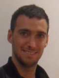
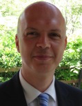
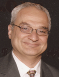
 Farhad
Mafie, SoC Conference Chairman. Farhad
Mafie, SoC Conference Chairman.
Moderator
Farhad Mafie, President and
CEO of Savant Company Inc., that provides marketing and business development
services to high-tech startups and mid-size companies on a worldwide basis.
He has over 25 years of experience in high-tech industries including
semiconductor and computer businesses; additionally, he has more than 15
years of university-level teaching experience.
In 2003, Farhad designed and
developed the annual Internationals System-on-Chip (SoC) Conference,
Exhibits, and Workshops. As the SoC Conference Chairman, he drives the
Conference leading-edge annual program.
As Chief Marketing Officer (CMO)
for a Switzerland startup, Farhad is driving an innovative mobile payment
system based on selected concepts that are very similar to Blockchain.
For almost six years at
Microsemi Corporation, as Vice President of Worldwide Product Marketing and
Corporate Communications teams (in US, EU, India, and China), Farhad
developed and managed the entire Microsemi’s worldwide outbound and inbound
marketing strategies and programs; and worked directly with executive team
on M&A projects and successfully integrating over 18 acquired companies.
Farhad is also the former Vice
President of Marketing/Business Development and Technical Sales Engineering
at Toshiba America Electronic Components, Inc. He was responsible for
marketing the entire Toshiba standard ICs in North America, as well as
engineering development for Toshiba's Embedded and Digital Consumer products
& solutions based on ASSP and SoC Models.
Farhad has worked at Lucent Technologies on marketing communications ICs,
Toshiba Information Systems on product definition for Toshiba's notebooks
PCs and handheld products, Unisys on designing new processors and computer
systems, Ocean Scientific on designing medical instrumentations, and MSI
Data on designing data collection products. He has a Master of Science and a
Bachelor of Science degree in Electronic Engineering from California State
University, Fullerton.
He is an author and a
translator. In 2003, he published the biography of Iranian poet and Nobel
nominee who lived in exile, Nader Naderpour (1929-2000), Iranian Poet,
Thinker, Patriot. Farhad is also Editor-in-Chief for the CRC Press SoC
Design and Technologies Book Series, which includes (1) Low-Power NoC for
High-Performance SoC Design and (2) Design of Cost-Efficient Interconnect
Processing Units. Farhad is an active member of IEEE, and he is the chair of
IEEE Orange County Solid-State Circuits Society (SSCS), as well as IEEE
Orange County Entrepreneurs' Network (OCEN). He is also a member of two UCI
Advisory Committees: Communication System Engineering and Embedded System
Engineering Certificate Programs.
|
|
|
|
Microchip
Technology

|
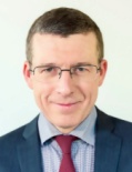
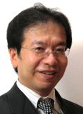
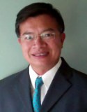
 Dr.
Lloyd Clark, Staff Applications Engineer, Microchip Technology. Dr.
Lloyd Clark, Staff Applications Engineer, Microchip Technology.
“MCU Cores and
Core-Independent Peripherals: Getting the Balance Right.”
Abstract: Modern 8-bit
microcontroller chips contain a capable, low-power CPU core as well as a
wide variety of peripherals that require minimal interaction with the CPU.
An increasing number of these peripherals are being designed to function as
autonomous units that can communicate with each other via direct paths that
do not involve the CPU -- so-called Core-Independent Peripherals (CIPs). By
communicating directly, these peripherals can perform tasks such as waveform
generation, analog-to-digital conversion with computation, and even
closed-loop control with little or no CPU interaction, allowing the CPU to
sleep or focus on other tasks. CIP implementations can provide significant
advantages such as a nearly-instantaneous response time since there is no
dependency on CPU interrupt latency. However, programming and debugging CIPs
can also be challenging because their activities are, by design, highly
independent of the CPU. What, then, is the proper partitioning of complexity
between the CPU core and CIPs? How does one get the balance right? This talk
will focus on some of the considerations involved in answering these
questions.
Bio: Lloyd Clark is currently a Staff Applications Engineer with Microchip
Technology. He has a decade of integrated circuit and MCU design experience
with Atmel. Prior to that, he was with Ticom Geomatics and Schlumberger
doing system design and embedded systems engineering, so he has worked with
SoCs both on the inside and outside. He has a Ph.D. in Electrical
Engineering and Computer Science from MIT and holds 7 U.S. patents.
|
|
|
|
University
of Bologna
 |
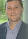
 Dr.
Davide Rossi, University of Bologna. Dr.
Davide Rossi, University of Bologna.
“PULP: A Transprecision
Multi-Core Platform for Micropower In-Sensor Analytics.”
Abstract: The “internet of
everything” envisions trillions of connected objects loaded with
high-bandwidth sensors requiring massive amounts of local signal processing,
fusion, pattern extraction and classification. From the computational
viewpoint, the challenge is formidable and can be addressed only by pushing
computing fabrics toward massive parallelism and tunable-precisions,
achieving brain-like energy efficiency levels. In this talk, I will describe
the evolution of the open source Parallel-Ultra-Low-Power (PULP) platform
and tackle the main challenges for next generation mW-range energy efficient
computing systems.
Bio: Davide Rossi, received the PhD from the University of Bologna, Italy,
in 2012. He has been a post doc researcher in the Department of Electrical,
Electronic and Information Engineering “Guglielmo Marconi” at the University
of Bologna since 2015, where he currently holds an assistant professor
position. His research interests focus on energy efficient digital
architectures in the domain of heterogeneous and reconfigurable multi and
many-core systems on a chip. This includes architectures, design
implementation strategies, and runtime support to address performance,
energy efficiency, and reliability issues of both high end embedded
platforms and ultra-low-power computing platforms targeting the IoT domain.
In these fields, he has published more than 60 paper in international
peer-reviewed conferences and journals.
|
|
|
|
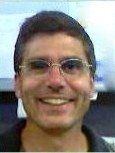
Kalray
 |
 Dr.
Benoît De Dinechin, Chief Technology Officer of Kalray. Dr.
Benoît De Dinechin, Chief Technology Officer of Kalray.
“Kalray’s MPPA3 Manycore
Processor: At the Heart of Intelligent Systems.”
Abstract: Kalray’s MPPA3
manycore processor is designed as a building block for intelligent systems.
Intelligent systems require the integration of high-integrity functions,
such as control-command, and high-performance functions, in particular
signal processing, image processing and machine learning. Such intelligent
systems are found in defense, aerospace, and automated vehicles. The MPPA3
processor will be taped-out in TSMC 16FFC technology by the end of 2018. The
MPPA3 architecture comprises multiple compute units connected by on-chip
global fabrics to external memory systems and network interfaces. Selecting
compute units composed of fully programmable cores, a large local memory and
an asynchronous data transfer engine enables to match the high performance
and energy efficiency of GPGPU processors, while avoiding their limitations.
We illustrate in particular how the MPPA3 processor accelerates deep
learning inference by distributing computations across compute units and
cores, and by offloading tensor operations to the tightly coupled
coprocessor connected to each core.
Bio: Benoît Dupont de Dinechin is Chief Technology Officer of Kalray. He is
the Kalray VLIW core main architect, and the co-architect of the
Multi-Purpose Processing Array (MPPA) processors. Benoît also defined the
Kalray software tools roadmap and contributed to its implementation. Before
joining Kalray, Benoît was in charge of Research and Development of the
STMicroelectronics Software, Tools, Services division, and was promoted to
STMicroelectronics Fellow in 2008. Prior to STMicroelectronics, Benoît
worked at the Cray Research park (Minnesota, USA), where he designed the
software pipeliner of the Cray T3E production compilers. Benoît earned an
engineering degree in Radar and Telecommunications from the Ecole Nationale
Supérieure de l'Aéronautique et de l'Espace (Toulouse, France), and a
doctoral degree in computer systems from the University Pierre et Marie
Curie (Paris) under the direction of Prof. P. Feautrier. He completed his
post-doctoral studies at the McGill University (Montreal, Canada) at the
ACAPS laboratory led by Prof. G. R. Gao.
|
|
|
|
Morning Break |
Morning Break |
|
|
|
IHS Markit Technology

|
 Tom
Hackenberg, Principal Analyst, Embedded Processors Technology, Media &
Telecom. Tom
Hackenberg, Principal Analyst, Embedded Processors Technology, Media &
Telecom.
“Next Generation SoCs, SiPs and PoPs – Markets driving new levels of
integration.”
Abstract: The scope of this presentation would be to demonstrate how
specific market demands have recently shaped the need for application
specific SoCs and how new technologies and trends, especially in an
automated world, are likely to further drive integration producing more
complex heterogeneous SoCs, and where that makes sense. The content would
run through six major market sectors Automotive, Consumer, Data Processing,
Industrial, Wired Communications and Wireless Communications. The intent is
to look at IoT, Edge Computing and AI enabling more advanced automation as
trends driving particular applications to benefit from even higher levels of
integration. AI, Machine Learning, Deep Learning, Storage/Data Centers,
Autonomous Vehicles, Neuromorphic Computing, Robotics, IoT, Blockchain,
Smart Home, Security, Aerospace Electrification, 5G Communications, H2M, and
Industry 4.0 would all be addressed where they are applicable by market.
Bio: Tom Hackenberg is the
principal analyst for embedded processor markets at IHS Markit. His broad
scope of processor coverage includes microcontrollers (MCU), microprocessors
(MPU), signal processors (DSP) and logic component markets. In addition to
component coverage, Tom provides a breadth of knowledge related to deeply
embedded systems in markets such as automotive, industrial and
telecommunications equipment. His analysis extends to processor technology
trends such as embedded vision, machine to machine (M2M) communications,
internet-of-things (IoT), sensor fusion, smart devices and embedded
security. As part of his research scope, Tom authors a detailed tracking
service for MCUs as well as custom reports on processors in automotive,
telecommunications and industrial markets. He supports IHS Markit core
services such as the Competitive Landscape Tool and Application Market
Forecast Tool. Tom is well versed in all processor components including
CPUs, GPUs, MPUs, MCUs, ASICs & ASSPs, FPGAs and configurable processors.
Tom has been providing embedded processing market analysis since 2006. He
holds a Bachelor of Science in Electrical Engineering from the University of
Texas at Austin specializing in processors and FPGAs.
|
|
|
|
NXP Semiconductor
Keynote

|
 Dr.
Robert Oshana, Vice President Software Engineering Research and Development,
Microcontroller Group. Dr.
Robert Oshana, Vice President Software Engineering Research and Development,
Microcontroller Group.
"RISC-V; is this the Linux
of CPU’s?"
Abstract: RISC-V is a free and
open ISA enabling a new era of processor innovation through open standard
collaboration. The RISC-V Foundation now has more than 100 member
organizations building the first open, collaborative community of software
and hardware innovators powering innovation at the edge forward. The RISC-V
ISA delivers a new level of software and hardware freedom on architecture in
an open extensible way. This open ISA delivers easier support from a broad
range of operating systems, software vendors and tool developers. The open
source of hardware, RISC-V does not rely on a single supplier, but instead
multiple suppliers, which supports unlimited potential for future growth.
Can RISC-V become the Linux of CPU’s. Can we achieve the freedom that exists
in the Free and Open Source Software (FOSS) community. We will discuss some
of the similarities as well as challenges in achieving such a model.
Bio:
Rob Oshana is Vice President of Software Engineering R&D for the
Microcontroller business line at NXP. He is a Senior Member IEEE and serves
on multiple industry advisory boards, including the RISC-V Board of
Directors. Rob is an recognized international speaker and has published
numerous books and papers on software engineering and embedded systems. He
is an adjunct professor at the University of Texas and Southern Methodist
University.
|
|
|
|
Lunch |
Lunch |
|
|
|
ON Semiconductor
Keynote

|
 Dr.
Hans Stork, Senior Vice President and Chief Technology Officer (CTO), ON
Semiconductor. Dr.
Hans Stork, Senior Vice President and Chief Technology Officer (CTO), ON
Semiconductor.
"Autonomous driving: where
distributed and local systems find their optimum configuration"
Abstract: The benefits
of improved cost and reliability have long been the driver of monolithic
integration. Individual devices are powered today by SoCs built in 10nm or
better process technologies. With lithography continuing to improve, further
digitization can be expected. Most of the functions that can be mapped into
the digital domain, should be integrated monolithically. However, any
associated memories require their own process and should be integrated at
the board or package level to satisfy bandwidth and power constraints. When
it comes to sensors or actuators, the unique processes are not compatible
with the low voltage digital domain. Fortunately, stacking of dies and
wafers has become practical, and provides much upside to optimizing each
process for its main function, whether that be photon capture, or power
control or management. In other words for sensor and actuator functions, SiP
is a key method to integrate heterogeneous processes into the smallest,
cheapest, highest performance packages. We will illustrate a few examples to
highlight the varied requirements and choices: from image sensors for
autonomous driving applications that require high dynamic range, at high
speed, and high pixel density, to intelligent motor control with local,
efficient power conversion using both discrete and mixed-signal processes
and devices.
TBD.
Bio: Dr. Hans Stork is Senior
Vice President and Chief Technology Officer (CTO) at ON Semiconductor. He
oversees the development of wafer process technologies, modeling and design
kits, design libraries, as well as packaging technologies and assembly
support. Prior to joining ON Semiconductor, Dr. Stork was Group Vice
President and CTO of the Silicon Systems Group at Applied Materials. From
2001 to 2007 he was Senior Vice President and the CTO of Texas Instruments.
Before that, Dr. Stork held various R&D and management positions at Hewlett
Packard Laboratories and at IBM’s T.J. Watson Research Center. Dr. Stork
serves on the supervisory board of ASML, is a member of the Scientific
Advisory board at IMEC, and has previously served on the boards of Sematech
and the SRC. He is also a longstanding member of the SIA Technology Strategy
Committee. He authored more than 100 cited papers and holds 11 U.S.
patents. He was elected IEEE Fellow in 1994, and served on several IEEE
sponsored conference program committees, and is currently vice-chair of the
Technical Field Awards Council and a member of the Awards Policy and
Portfolio Review Committee. Dr. Stork was born in Soest, The
Netherlands, and received the Ingenieur degree in electrical engineering
(EE) from Delft University of Technology, Delft, The Netherlands, and holds
a PhD in EE from Stanford University.
|
|
|
|
Intel
 |
 Jeff
Parkhurst, PhD – Center Director for the Intel Science and Technology Center
on Agile HW Design. Jeff
Parkhurst, PhD – Center Director for the Intel Science and Technology Center
on Agile HW Design.
“Agile HW Design: Exploring
the application of Agile SW methods to HW design.”
Abstract: Intel has been
working with UC Berkeley and Stanford on applying Agile SW methods to HW
design via the Intel Science and Technology Center (ISTC) on Agile HW Design
including exploring increasing front end design productivity. This talk will
cover some of the efforts in this center and survey some key learnings.
Bio: Dr. Jeff Parkhurst is the Program Director for the Intel Science and
Technology Centers on Agile HW Design. He is responsible for managing the
operational details in each center as well as providing direction setting of
the research. The Center Director is the primary liaison between Intel and
the universities on all operational matters including contracts, IP, space,
logistics, funding, and technology/knowledge transfer. Center director is
also responsible for guiding research and messaging. Prior to this
assignment, Jeff was program director for the Intel Science and Technology
center on Big Data. Jeff was also an Academic Research Programs Manager
working with senior technologists internal and external to Intel setting
research directions for the design science areas of the Semiconductor
Research Corporation (SRC). Jeff received his BS from University of Nevada
at Reno in 1983 and his MS from the University of California at Davis in
1988 and his PhD at Purdue University in 1994. Dr. Parkhurst is the author
of numerous papers and one patent.
|
|
|
|
Microsemi

|
 Dr.
Rino Micheloni, Vice-President and Fellow, Microsemi Corporation. Dr.
Rino Micheloni, Vice-President and Fellow, Microsemi Corporation.
“Scaling and Reliability challenges of 3D NAND Flash memories.”
Abstract: Over the last 2 decades, NAND Flash memories have changed
our lives: Flash cards have almost completely replaced photographic films,
and USB-pens have driven floppy disks to extinction. In the last few years,
thanks to a great balance between cost and performances (i.e. write and read
speeds), NAND Flash technology, in the form of Solid State Drives (SSDs),
has begun gaining momentum over Hard Disk Drives (HDDs). This is especially
true in consumer electronics, but SSD’s penetration in enterprise and cloud
applications seems unstoppable. 3D NAND Flash is a brand-new technology, not
only because of its multi-layer architecture, but also because it is based
on a new type of NAND memory cell. There is a plethora of different
materials and vertical architectures out there. New cells, new materials,
new vertical architectures; basically, each Flash vendor has its unique
solution. To increase the number of Gbit per mm2, cell’s size should shrink
and the number of layers must go up, causing a lot of manufacturing
challenges. Not only that. Indeed, NAND reliability becomes a major concern,
especially when looking at SSD applications, where Flash is used as a
standard drive. Therefore, together with the technological effort, Flash
microcontrollers have to be designed to tolerate more and more native errors
coming from the NAND (i.e. raw Bit Error Rate, BER).
Bio: Dr. Rino Micheloni is Vice-President and Fellow at Microsemi
Corporation, where he currently runs the Flash Signal Processing Labs in
Milan, Italy, with special focus on NAND Flash, Error Correction Codes, and
Machine Learning. Prior to joining Microsemi, he was Fellow at PMC-Sierra,
working on NAND Flash characterization, LDPC, and NAND Signal Processing as
part of the team developing Flash controllers for PCIe SSDs. Before that, he
was with IDT (Integrated Device Technology) as Lead Flash Technologist,
driving the architecture and design of the BCH engine in the world’s first
PCIe NVMe SSD controller. Early in his career, he led NAND design teams at
STMicroelectronics, Hynix, and Infineon/Qimonda; during this time, he
developed the industry’s first MLC NOR device with embedded ECC technology
and the industry’s first MLC NAND with embedded BCH. Dr. Micheloni is IEEE
Senior Member, he has co-authored more than 70 publications, and he holds
278 patents worldwide (including 131 US patents). He received the
STMicroelectronics Exceptional Patent Award in 2003 and 2004, and the
Infineon/Qimonda IP Award in 2007. Dr. Micheloni has published the following
books with Springer: Solid-State-Drives (SSDs) Modeling (2017), 3D Flash
Memories (2016), Inside Solid State Drives (2013), Inside NAND Flash
Memories (2010), Error Correction Codes for Non-Volatile Memories (2008),
Memories in Wireless Systems (2008), and VLSI-Design of Non-Volatile
Memories (2005).
|
|
|
|
Afternoon Break |
Afternoon Break |
|
|
|
Fujitsu
Semiconductor Limited.
 |
 Hitoshi
Saito, director of Emerging memory Department of Fujitsu Semiconductor
Limited. Hitoshi
Saito, director of Emerging memory Department of Fujitsu Semiconductor
Limited.
“Highly reliable
non-volatile memory suitable for battery-less equipment and its business
solutions.”
Abstract: Ferroelectric random access memory (FRAM) is a non-volatile memory
which has advantages such as high write endurance, low power consumption,
high writing speed, verification-free, and stronger data retention even in
the high temperature environment in comparison with conventional
non-volatile memories. Although a downside of our previously commercialized
FRAM was large cell, we have newly developed a triple hydrogen protection
structure which can thoroughly protect PZT capacitor from hydrogen
degradation and reduce the area to 40%. [1] FRAM is suitable for the
battery-less equipment operated by energy harvesting because of the low
power consumption of FRAM. For example, we have proposed a FRAM-embedded
wearable solution, namely “smart shoes”. That can record data of step counts
using accelerometer and send it to a smart phone or a smart watch using weak
electric power unstably generated by bending soles integrated in the smart
shoes. Moreover, an FRAM-embedded battery-less keyboard can communicate with
computer or tablet with reader/writer in the same way as radio frequency
identification (RFID) tags communicating. A new non-volatile RAM, so called
Nanotube RAM (NRAM) consisting of carbon nanotube (CNT) cell resistor is
under developing for higher density memory portfolio. We can apply NRAM to
fine pitch logic process and continue shrinkage. Because NRAM has high
endurance up to 1E12 cycles [2], high retention ability at 300 degree C [3],
and high speed writing, a high-density NRAM has potential to replace NOR
FLASH and even DRAM used in the mobile devices such as a smart phone. We
also continue to promote the numbers of business solutions using new
non-volatile RAMs, those offer a low power consumption, and many other
advantages. I will present our strategy for the future non-volatile RAM in
its development and marketing.
1. H. Saito et al., IEEE 7th IMW, 137 (2015).
2. S. Ning et al., IEEE T. Electron Devices, 2837 (2015).
3. T. Rueckes, Flash Memory Summit, 303 (2011).
Bio: Hitoshi Saito received
the bachelor of engineering degree in electrical engineering from Tokyo
University of Agriculture and Technology, Tokyo, Japan and joined FUJITSU
LIMITED in 1990. He had contributed to development of DRAM and FLASH process
technology in 0.6 μm to 0.13 μm, had developed FRAM process and device of
0.35 μm to 0.18 μm technology, then has been developing NRAM process and
device of 180 nm to 55 nm technology. Since 2016, he has been a director of
Emerging memory Department of FUJITSU SEMICONDUCTOR LIMITED. His recent
interest is nonvolatile memory process and device including future exotic
memories.
|
|
|
|
Mythic
 |
 Dr.
Dave Fick, CTO and co-Founder of Mythic. Dr.
Dave Fick, CTO and co-Founder of Mythic.
“Edge Inference with Matrix
Multiplying Memories.”
Abstract: Deep neural networks
and deep learning have already shown a tremendous ability to serve as the
foundation for highly-advanced perceptual algorithms. They will be essential
for the most important technological developments over the next 10 years:
autonomous systems (cars, drones, last-mile delivery), factory robotics, AR/VR,
security, smart-buildings, and IoT to name a few. One of the major
challenges of realizing this future falls on the semiconductor industry:
delivering the massive compute performance needed for real-time neural
networks in a form-factor suitable for devices with size, power, and cost
constraints. When faced with massive compute loads and tough real-time
requirements, the challenges come down to: performance (both throughput and
latency), power dissipation, cost, and ease of integration. In deep neural
networks (DNNs), the limiting factor is memory. The actual arithmetic itself
is quick and low power: DNNs operate primarily on simple arithmetic like
multiplies and additions and bit-depths are low (especially for inference).
The challenge is memory: getting neural network weights, which can exceed 50
million, to the right processing element at the right time to be multiplied
against the input and intermediate data. Mythic created significant
advantages for inference compute using flash memory and analog computation.
Flash is capable of storing many levels (up to 8-10 bits) if it is treated
as a short term (10-30 days) memory rather than a long term (10 years at 125
°C) memory. This represents an on-chip storage medium that is 50x denser
than SRAM. Normally reading 8 bit multi-level-cell values out of flash would
be very time and energy consuming. The solution is analog computation:
calibrated analog currents that are steered across a string of flash
transistors and modulated by the stored threshold voltages. This effectively
performs the matrix math of DNN inference in a massively parallel fashion at
low voltages, without ever having to read multi-level values out of the
cells. Keeping processors close to memory is key, and by turning the flash
cells into multiply-accumulate units, there is no way to make them closer.
The results speak for themselves: a single chip consuming under 2 Watts of
power can deliver the same framerate for Resnet-50 as a $1000 GPU burning
150 Watts – at a small fraction of the price. More advanced networks, such
as OpenPose and Video/LIDAR, can run at 60 fps at 2.5 W on two Mythic chips
connected together. The same $1000 GPU burns 250 W running the same
networks. These performance numbers will ensure the future of AI in
applications like autonomous vehicles don’t have to live inside of $5000
liquid cooled boxes.
Bio: Dave Fick is the CTO and
co-founder of Mythic, an Austin-based startup that is creating the next
generation of inference microchips. Mythic uses mixed-signal computing to
achieve 20-100x improvements in neural network performance for edge devices,
and has raised $55M from top-tier investors to execute on this vision. Dave
Fick earned his Ph.D. from the University of Michigan.
|
|
|
|
University of California,
Irvine
(UCI)
Keynote
 |
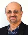 Nader
Bagherzadeh, Professor (Joint Appointment), Electrical Engineering and
Computer Science & Donald Bren School of Information and Computer Science. Nader
Bagherzadeh, Professor (Joint Appointment), Electrical Engineering and
Computer Science & Donald Bren School of Information and Computer Science.
"Machine Learning a Paradigm
Shift but has Limitations."
Abstract: In this talk,
an overview of current trends in machine learning will be discussed with an
emphasize on challenges and opportunities. Finally, there will be an
overview of our work related to this topic of research.
Bio: Dr. Nader Bagherzadeh has
been involved in research and development in the areas of computer
architecture, reconfigurable computing, VLSI chip design, and computer
graphics. For almost ten years ago, he was the first researcher working on
the VLSI design of a Very Long Instruction Word (VLIW) processor. Since
then, he has been working on multithreaded superscalars and their
application to signal processing and general purpose computing. His current
project at UC, Irvine is concerned with the design of coarse grain
reconfigurable pixel processors for video applications. The proposed
architecture, called MorphoSys, is versatile enough to be used for digital
signal processing tasks such as the ones encountered in wireless
communications and sonar processing. DARPA and NSF fund the MorphoSys
project (total support $1.5 million). Dr. Bagherzadeh was the Chair of
Department of Electrical and Computer Engineering in the Henry Samueli
School of Engineering at University of California, Irvine. Before joining
UC, Irvine, from 1979 to 1984, he was a member of the technical staff (MTS)
at AT&T Bell Laboratories, developing the hardware and software components
of the next-generation digital switching systems (#5 ESS). Dr. Bagherzadeh
holds a Ph.D. in computer engineering from The University of Texas at
Austin. As a Professor, he has published more than a hundred articles in
peer-reviewed journals and conference papers in areas such as advanced
computer architecture, system software techniques, and high performance
algorithms. He has trained hundreds of students who have assumed key
positions in software and computer systems design companies in the past
twelve years. He has been a Principal Investigator (PI) or Co-PI on more
than $2.5 million worth of research grants for developing next-generation
computer systems for solving computationally intensive applications related
to signal and image processing.
|
|
|
|
Panel
|
Panel:
“AI and
Machine Learning driving the Intelligent Machines: Will the Technological
Singularity Happen?"
Abstract: Artificial intelligence (AI) will no doubt have a
significant impact on society in the coming years. But how intelligent can a
machine be? The idea that human history is approaching a “Technological
Singularity” that ordinary humans will someday be overtaken by artificially
intelligent machines has moved from the realm of science fiction to serious
debate. Some singularity theorists predict that if the field of AI and
machine learning continues to develop at its current dizzying rate, the
singularity could come about in the middle of the present century. This
panel will discuss the current state of the art for AI, deep learning and
robotics, and try to predict where this technology is heading.
Moderator: Farhad Mafie, SoC Conference Chairman.
Panelists:
1.
Professor Alexander Ihler, Associate Professor, Information & Computer
Science, UC Irvine.
2. Anil Mankar, COO & SVP Engineering, BrainChip Inc.
3. Geeta Chauhan, CTO, DeepCloud.
4. Manoj
Roge, VP, Strategic Planning & Business Development, Achronix.
5. Nader
Bagherzadeh, Professor (Joint Appointment), Electrical Engineering and
Computer Science & Donald Bren School of Information and Computer Science.
University of California, Irvine.
6. TBA.
This
Panel Is Open To Everyone . . .
Register Online for FREE Panel Pass
|
|
|
|
Savant
Company Inc.
SoC Conference


 |
Farhad
Mafie, SoC Conference Chairman.
Moderator
Farhad Mafie, President and
CEO of Savant Company Inc., that provides marketing and business development
services to high-tech startups and mid-size companies on a worldwide basis.
He has over 25 years of experience in high-tech industries including
semiconductor and computer businesses; additionally, he has more than 15
years of university-level teaching experience.
In 2003, Farhad designed and
developed the annual Internationals System-on-Chip (SoC) Conference,
Exhibits, and Workshops. As the SoC Conference Chairman, he drives the
Conference leading-edge annual program.
As Chief Marketing Officer (CMO)
for a Switzerland startup, Farhad is driving an innovative mobile payment
system based on selected concepts that are very similar to Blockchain.
For almost six years at
Microsemi Corporation, as Vice President of Worldwide Product Marketing and
Corporate Communications teams (in US, EU, India, and China), Farhad
developed and managed the entire Microsemi’s worldwide outbound and inbound
marketing strategies and programs; and worked directly with executive team
on M&A projects and successfully integrating over 18 acquired companies.
Farhad is also the former Vice
President of Marketing/Business Development and Technical Sales Engineering
at Toshiba America Electronic Components, Inc. He was responsible for
marketing the entire Toshiba standard ICs in North America, as well as
engineering development for Toshiba's Embedded and Digital Consumer products
& solutions based on ASSP and SoC Models.
Farhad has worked at Lucent Technologies on marketing communications ICs,
Toshiba Information Systems on product definition for Toshiba's notebooks
PCs and handheld products, Unisys on designing new processors and computer
systems, Ocean Scientific on designing medical instrumentations, and MSI
Data on designing data collection products. He has a Master of Science and a
Bachelor of Science degree in Electronic Engineering from California State
University, Fullerton.
He is an author and a
translator. In 2003, he published the biography of Iranian poet and Nobel
nominee who lived in exile, Nader Naderpour (1929-2000), Iranian Poet,
Thinker, Patriot. Farhad is also Editor-in-Chief for the CRC Press SoC
Design and Technologies Book Series, which includes (1) Low-Power NoC for
High-Performance SoC Design and (2) Design of Cost-Efficient Interconnect
Processing Units. Farhad is an active member of IEEE, and he is the chair of
IEEE Orange County Solid-State Circuits Society (SSCS), as well as IEEE
Orange County Entrepreneurs' Network (OCEN). He is also a member of two UCI
Advisory Committees: Communication System Engineering and Embedded System
Engineering Certificate Programs.
|
|
|
|
BrainChip
|
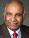 Anil
Mankar, COO & SVP Engineering, BrainChip Inc. Anil
Mankar, COO & SVP Engineering, BrainChip Inc.
Panelist.
Bio: Anil Mankar has spent 30
years developing products in the semiconductor industry. At Western Digital,
Mr. Mankar developed PC core Logic chipsets. During his years at Conexant
Systems Inc. in the position of VP of Engineering, he developed multiple
products across industry segments and later became the company’s Chief
Development Officer overseeing all product development for V92 Modem, DSL,
Set-top boxes, PC audio and video ‘System on a Chip’ products. Mr. Mankar
was SVP of VLSI Engineering at Mindspeed Technologies, responsible for
Wireless and VOIP infrastructure product development.
|
|
|
|
UC Irvine
|
 Professor
Alexander Ihler, Associate Professor, Information & Computer Science, UC
Irvine. Professor
Alexander Ihler, Associate Professor, Information & Computer Science, UC
Irvine.
Panelist.
Bio: TBA.
|
|
|
|
DeepCloud
|
 Geeta
Chauhan, CTO, DeepCloud. Geeta
Chauhan, CTO, DeepCloud.
Panelist.
Bio: CTO with 25 yrs of
expertise in building resilient, anti-fragile, large scale distributed
platforms with 1B+ users for startups and Fortune 500s. Built and launched
15+ platforms and countless applications based on AI/Deep Learning, Cloud
Computing, Blockchain, SDN, Micro-services, Self-healing, Elastic Scaling.
Lead diverse global teams, scaling complex distributed systems for companies
ranging from nimble startups to Fortune 500s. Focusing these days on
building AI, Deep Learning and Blockchain based platforms for startups. Or
tinkering in my garage to convert my electric car to run autonomously.
|
|
|
|
Achronix
|
 Manoj
Roge, VP, Strategic Planning & Business Development, Achronix. Manoj
Roge, VP, Strategic Planning & Business Development, Achronix.
Panelist.
Bio: TBA.
|
|
|
|
University of California,
Irvine
(UCI)
|
Nader
Bagherzadeh, Professor (Joint Appointment), Electrical Engineering and
Computer Science & Donald Bren School of Information and Computer Science.
Panelist.
Bio: Dr. Nader Bagherzadeh has
been involved in research and development in the areas of computer
architecture, reconfigurable computing, VLSI chip design, and computer
graphics. For almost ten years ago, he was the first researcher working on
the VLSI design of a Very Long Instruction Word (VLIW) processor. Since
then, he has been working on multithreaded superscalars and their
application to signal processing and general purpose computing. His current
project at UC, Irvine is concerned with the design of coarse grain
reconfigurable pixel processors for video applications. The proposed
architecture, called MorphoSys, is versatile enough to be used for digital
signal processing tasks such as the ones encountered in wireless
communications and sonar processing. DARPA and NSF fund the MorphoSys
project (total support $1.5 million). Dr. Bagherzadeh was the Chair of
Department of Electrical and Computer Engineering in the Henry Samueli
School of Engineering at University of California, Irvine. Before joining
UC, Irvine, from 1979 to 1984, he was a member of the technical staff (MTS)
at AT&T Bell Laboratories, developing the hardware and software components
of the next-generation digital switching systems (#5 ESS). Dr. Bagherzadeh
holds a Ph.D. in computer engineering from The University of Texas at
Austin. As a Professor, he has published more than a hundred articles in
peer-reviewed journals and conference papers in areas such as advanced
computer architecture, system software techniques, and high performance
algorithms. He has trained hundreds of students who have assumed key
positions in software and computer systems design companies in the past
twelve years. He has been a Principal Investigator (PI) or Co-PI on more
than $2.5 million worth of research grants for developing next-generation
computer systems for solving computationally intensive applications related
to signal and image processing.
|
|
|
|
Networking |
Student Design Contest &
Networking
|
|
|
|
|
Day TWO Thursday, October 18, 2018
SoC Conference Program Agenda* |
|
|
|
Savant
Company Inc.
SoC Conference |
Farhad
Mafie, SoC Conference Chairman.
Moderator
Farhad Mafie, President and
CEO of Savant Company Inc., that provides marketing and business development
services to high-tech startups and mid-size companies on a worldwide basis.
He has over 25 years of experience in high-tech industries including
semiconductor and computer businesses; additionally, he has more than 15
years of university-level teaching experience.
In 2003, Farhad designed and
developed the annual Internationals System-on-Chip (SoC) Conference,
Exhibits, and Workshops. As the SoC Conference Chairman, he drives the
Conference leading-edge annual program.
As Chief Marketing Officer (CMO)
for a Switzerland startup, Farhad is driving an innovative mobile payment
system based on selected concepts that are very similar to Blockchain.
For almost six years at
Microsemi Corporation, as Vice President of Worldwide Product Marketing and
Corporate Communications teams (in US, EU, India, and China), Farhad
developed and managed the entire Microsemi’s worldwide outbound and inbound
marketing strategies and programs; and worked directly with executive team
on M&A projects and successfully integrating over 18 acquired companies.
Farhad is also the former Vice
President of Marketing/Business Development and Technical Sales Engineering
at Toshiba America Electronic Components, Inc. He was responsible for
marketing the entire Toshiba standard ICs in North America, as well as
engineering development for Toshiba's Embedded and Digital Consumer products
& solutions based on ASSP and SoC Models.
Farhad has worked at Lucent Technologies on marketing communications ICs,
Toshiba Information Systems on product definition for Toshiba's notebooks
PCs and handheld products, Unisys on designing new processors and computer
systems, Ocean Scientific on designing medical instrumentations, and MSI
Data on designing data collection products. He has a Master of Science and a
Bachelor of Science degree in Electronic Engineering from California State
University, Fullerton.
He is an author and a
translator. In 2003, he published the biography of Iranian poet and Nobel
nominee who lived in exile, Nader Naderpour (1929-2000), Iranian Poet,
Thinker, Patriot. Farhad is also Editor-in-Chief for the CRC Press SoC
Design and Technologies Book Series, which includes (1) Low-Power NoC for
High-Performance SoC Design and (2) Design of Cost-Efficient Interconnect
Processing Units. Farhad is an active member of IEEE, and he is the chair of
IEEE Orange County Solid-State Circuits Society (SSCS), as well as IEEE
Orange County Entrepreneurs' Network (OCEN). He is also a member of two UCI
Advisory Committees: Communication System Engineering and Embedded System
Engineering Certificate Programs.
|
|
|
|
University
of Michigan

NASA JPL
 |
 Dr.
Mina Rais-Zadeh, Associate Professor, University of Michigan, EECS
Department, Technical Supervisor and Lead, Advanced Optical and
Electromechanical Microsystems, NASA JPL. Dr.
Mina Rais-Zadeh, Associate Professor, University of Michigan, EECS
Department, Technical Supervisor and Lead, Advanced Optical and
Electromechanical Microsystems, NASA JPL.
“"Phase Change RF and
Optoelectronics on Silicon."
Abstract: Chalcogenide
glasses are a sub-family of phase change materials (PCM) with nonvolatile
properties; familiar examples of chalcogenide glasses include Germanium
(Antimony) Telluride [1] and Vanadium Dioxide (VO2) [2]. For several
decades, chalcogenide glasses have been incorporated into different
electronic and optical systems. Certain properties of PCMs are especially
useful for such applications. Specifically, PCMs undergo a structural
transition between their room-temperature-stable phases, amorphous and
crystalline, in response to an external stimulus such as electrical current
or laser pulse. Amorphous films are optically transparent and electrically
isolative while crystalline PCMs are typically optically lossy, reflective,
and electrically conductive. More than six orders in magnitude of change in
the resistivity and 2X change in optical properties with reliable phase
transitions make Germanium Telluride (GeTe) a good candidate to be
incorporated in both electrical and optical devices. Moreover, as GeTe lacks
antimony, which is a contaminant that reduces stability, it is arguably a
better material for nanofabrication processing. One area for application of
PCMs is reconfigurable switches for radio frequencies (RF) with high
isolation. PCMs integrated in a band-pass filters have the potential to be
very useful in numerous of applications such as cognitive radios, modern
transceivers, anti-jamming communication systems, and multi-channel systems.
Electrical resistivity modulation between the amorphous and crystalline
phases of GeTe helps to improve switching at RF regions with very low
insertion losses and high isolations up-to 20 GHz in PCM-based RF switches
[3]. The core component of GeTe-based switches is the heating method
integrated in them for crystallographic phase transition. Among the
different methods of GeTe phase transition, joule-heating with an electrical
pulse either through direct or indirect heat sources stand apart as the
preferred method. This is due to easier integration and low cost, as well as
the availability of fast, reversible, and low power transitions for many
cycles. Potential applications of PCMs are not limited to RF applications
alone. Tunable optical components are of utmost interest in a variety of
applications such as shutters, modulators, and color filters. A nonvolatile
and ultra-high contrast optical switch is needed to isolate the laser beam
in a chip-scale atomic clock for higher accuracy. Incorporation of GeTe in a
Fabry–Pérot cavity, leads to realization of a zero static power color
reflector. A zero static power color reflector has the potential to
revolutionize commonly used static optical components to produce colors
[4-7]. Zero static power passive displays, which only consume power when
switching colors, are among most important alternatives to active devices,
especially in ultra-low power displays with a low refresh rate. Moreover,
continues vivid colors in a single pixel demonstration is only possible
where a tunable color reflector is integrated into the display system such
as in single mirror interferometrics (SMI), where a moving MEMS mirror is
used to tune the pixel color [8,9].
To address durability, power, and performance of these SMI devices, a GeTe-based
layered color reflector on silicon substrate is introduced. Ultra-thin GeTe
films used in these devices undergo a smoother phase transitions compared to
thicker films. Unlike VO2 or liquid crystal, these are stable at room
temperature without the presence of external stimuli [10,11]. Multiple total
light absorption layers consisting of ultra-thin layers of GeTe and silver
(Ag) are used to achieve such a tunable color reflector. Stacking the total
light absorption is possible with the availability of Ag films with
thicknesses < 20 nm Ag, developed by adding 3% of aluminum to during the
sputtering as well as as-sputtered amorphous silicon films with high optical
index [12]. Such a design can provide smaller time constant which is
required for successful amorphization process. To sum up, this paper
introduces a novel optical switch consist of a PCM material integrated with
noble metals and amorphous silicon to achieve tunable color filtering within
the visible spectrum employing a total light absorption phenomenon in thin
films with high loss.
[1] Hosseini, P., Wright, CD., and Bhaskaran, H., “An optoelectronic
framework enabled by low-dimensional phase-change films”. Nature, 511(7508),
pp. 206-211. (2014).
[2] Liu, M., et al. "Terahertz-field-induced insulator-to-metal transition
in vanadium dioxide metamaterial." Nature 487.7407 (2012): 345.
[3] Wang, M., 2017. “Phase Change Material Based Ohmic Switches for
Reconfigurable RF Applications.”, PhD dissertation, 2017, University of
Michigan.
[4] Li, J., et al. "Highly Efficient Organic Light‐Emitting Diode Based on a
Hidden Thermally Activated Delayed Fluorescence Channel in a Heptazine
Derivative." Advanced Materials 25.24 (2013): 3319-3323.
[5] Zhu, M., and Yang, C. "Blue fluorescent emitters: design tactics and
applications in organic light-emitting diodes." Chemical Society Reviews
42.12 (2013): 4963-4976.
[6] Lee, K.T., et al. "Strong Resonance Effect in a Lossy Medium‐Based
Optical Cavity for Angle Robust Spectrum Filters." Advanced Materials 26.36
(2014): 6324-6328.
[7] Do, Y. S., et al. "Plasmonic Color Filter and its Fabrication for
Large‐Area Applications." Advanced Optical Materials 1.2 (2013): 133-138.
[8] Lee, J., Chen, H. F., Batagoda, T., Coburn, C., Djurovich, P. I.,
Thompson, M. E., & Forrest, S. R. (2016). Deep blue phosphorescent organic
light-emitting diodes with very high brightness and efficiency. Nature
materials, 15(1), 92.
[9] Hong, J., Chan, E., Chang, T., Fung, T. C., Hong, B., Kim, C., ... & Wen,
B. (2015). Continuous color reflective displays using interferometric
absorption. Optica, 2(7), 589-597.S
[10] Jafari M. and Rais-Zadeh M., “Zero-static-power phase-change optical
modulator,” Optics letter, pp. 1177-1180. (2016).
[11] Jafari, M. and Rais-Zadeh, M., “A 1550 NM phase change electro-optical
shutter.” In IEEE 29th International Conference on Micro Electro Mechanical
Systems (MEMS), pp. 655-658. IEEE. (2016)
[12] Zhang, C., et al. "An ultrathin, smooth, and low‐loss Al‐doped Ag film
and its application as a transparent electrode in organic photovoltaics."
Advanced Materials 26.32 (2014): 5696-5701.
Bio: Mina Rais-Zadeh received the B.S. degree in electrical engineering from
Sharif University of Technology and M.S. and Ph.D. degrees both in
Electrical and Computer Engineering from Georgia Institute of Technology in
2005 and 2008, respectively. From 2008 to 2009, she was a Postdoctoral
Research Fellow at Georgia Institute of Technology. In 2009, she joined the
University of Michigan, Ann Arbor, as an Assistant Professor of Electrical
Engineering and Computer Science (EECS). Since 2014, she has been an
Associate Professor in EECS with courtesy appointment in the Department of
Mechanical Engineering. She is currently at NASA JPL and on leave of absence
from U. of Michigan. She is a senior member of IEEE, and a member of ASME,
and a distinguished lecturer of IEEE EDS. She has served as a member of the
technical program committee of IEEE IEDM (2011-2014), IEEE Sensors
Conference (2011-2017), the Hilton Head workshop (2012, 2014, 2016), the
IEEE MEMS Conference (2014-2015), Transducers (2015, 2017), and IFCS
(2015-2018). She served on the 2015 IEEE MEMS Executive Committee and was an
associate editor of IEEE Electron Device Letters (EDL). She is now an
associate editor for the IEEE Journal of Microelectromechanical Systems (JMEMS)
and on editorial board of Nature Scientific Reports. She is the TPC chair
for the Sensors, Actuators and Microsystems Workshop (Hilton Head) Workshop
in 2018. Her research interests include electron devices for wireless
communication and sensing applications and the related device physics,
resonant micromechanical devices, RF MEMS, gallium nitride MEMS, and micro/nano
fabrication process development.
|
|
|
|
Cadence Design Systems
 |
 Pankaj
Singh and Vinayak Hegde, Cadence Design Systems, Bangalore, India. Pankaj
Singh and Vinayak Hegde, Cadence Design Systems, Bangalore, India.
“Overcoming Challenges of Verifying Complex High Speed Mixed Signal
Designs."
Abstract:
Verification complexity of Interface Mixed Signal IP’s like
SERDES increased manifold with increased design. Receive (RX) path of the
SERDES is most complex and hence verifying it thoroughly is a significant
challenge. This includes verifying calibration techniques, equalization
adaptation algorithm, clock and data recovery path, production test-modes
like eye-surf form the core of receiver path verification of SERDES. As
verification of these techniques have strong link with analog parameters;
Verilog standard-logic functional models are not sufficient to ensure
thorough verification. Verification using Spice netlist is desirable to get
most accurate results, However this is not a practical approach as limiting
factor in this context is the longer simulation time. Efficient and
Innovative Digital Mixed-Signal (DMS) verification methodology is required
to enable effective verification of RX path of SERDES. This presentation
describes the usage of Real value models and Capture -Verify approach to
verify complex high speed mixed signal design. Real value models are the
backbone of DMS methodology. Real value models are created for all critical
modules in Receive path like Equalizer and Sampler and its associated
peripheral modules. It is critical to make sure created models are
functionally equivalent to respective designs. This is achieved by verifying
each created model with respective designs for all functional modes. While
the Real Value models are effective in meeting overcoming the simulation
performance bottleneck by achieving 10x faster simulation time; the
Nonlinearity factors of the front-end design are not represented accurately
in discrete domain real value models for next generation of SerDes Design at
very high data rate. To overcome this problem, a novel approach called
‘capture and verify’ is used for verifying the jitter tolerance and eye
parameters. In this approach, waveforms from spice level verification of
Equalizer for different functional modes are captured and stored. These
stored waveforms are used to generate run time table-based models to
accurately represent the analog modules. These run time models are used in
top-level simulations along with real value models thereby achieving
required goal of simulation performance without compromising on accuracy of
results. The complete Design Verification (DV) environment is developed
using UVM-e Methodology. Verification environment contains model for
transmitter with all de-emphasis settings along with protocol compliant
channels with multiple attenuations. DV infrastructure has hooks to plug-in
required channel models to verify SERDES. This verification environment is
also capable of verifying the clock data recovery (CDR) path of the design
using protocol compliant jitter and Spread-Spectrum Clocking (SSC) stimulus.
The real value modelling bridges the gap between the performance
requirements of the simulation and accuracy limitations of design. A
significant speed-up in simulation performance is achieved (almost 10X in
this case) by replacing with functionally equivalent real value models for
mixed signal designs. Usage of Capture and Verify methodology with spice
simulation waveforms for critical blocks ensures non-linearity of the next
generation high speed SerDes design is well captured in simulations provide
complete comprehensive solution for high speed mixed signal designs.
Sampler and Equalizer calibration results are shown in Figure 1. Here static
calibration is followed by Adaptation and Dynamic Offset Correction. Offset
values can be dynamically configured from verification environment to cover
all the required ranges. Figure 2 shows the results of CDR path verification
with 4000 ppm offset, 1MHz single tone sine jitter for data rate of 5 Gbps.
Final paper will cover more details on DMS verification
challenges and the verification methodology for different calibration
techniques, 2D Eye surf and CDR path verification with jitter, SSC stimulus.
Bio/s: Vinayak Hegde is Sr Design Engineering Manager in IP
group of Cadence Design Systems, Bangalore. He is responsible for Modelling
and Mixed Signal verification of SerDes IP’s in Bangalore Center. He has
more than 16 years of experience in mixed signal verification and ams
methodology development since he graduated from Karnataka University,
Dharwar, India. He also holds a Master of Science degree in
Microelectronics from BITS, Pilani, India. He has 5 international
presentations to his name in DVCon India, DVCon US and DAC.
Pankaj completed his Bachelors in Electronics from NIT Bhopal
in 1993; Master's in Electrical Engineering from USF, Florida and an MBA
from SMU, Dallas. He has 20+ years of industry experience which includes
various leadership management roles. Currently he is leading and managing
Central Verification R&D teams for Cadence Design Systems India and APAC. He
has published 30 technical papers in various international conferences.
|
|
|
|
TSI Semiconductors.

|
 Wilbur
Catabay, SVP TDCS & Corporate Strategy, TSI Semiconductors. Wilbur
Catabay, SVP TDCS & Corporate Strategy, TSI Semiconductors.
"Leveraging 0.18UM
Foundry Technologies with Heterogeneous Integration of Novel Devices in an
ITAR/Trusted Foundry."
Abstract: There has been rapid growth in our Consumer and Industrial markets
that is driving the need for more sensors and big data to fulfill the needs
of innovative ideas that push the limits beyond what a typical foundry can
offer. Today’s IOT devices are getting smarter and more connected and is now
moving to the next stages of the “Internet of Everything”. Devices for RFID
tags, Micro controller, NVM, DNA sequencing and MEMS Sensors have been
around but are constantly evolving and are considered as significant and
innovative changes to our devices. Silicon innovators in Large Device
Manufacturers, small to mid size companies, and start-up companies with
disruptive technologies targeting today's "Smart Markets" need a flexible
fabrication facility to showcase a proof of concept and if successful, a
place to commercialize the technology with secure IP protection and more
importantly IP retention. TSI Semiconductors will give an overview of how to
close the innovation gap to enable these disruptive technologies by
integrating and leveraging the CMOS platform with new materials and novel
architectures in a high volume manufacturing facility.
Bio: Wilbur Catabay is a veteran of the semiconductor industry with more
than 25 years of experience. Recently, Mr. Catabay was VP of Technology at
SVTC Technologies and President of Silicon Integrated Solutions, Inc., who
provided Engineering Services for Device and Process Integration. He also
was Senior Director for LSI Logic’s Foundry Engineering & Integration
organization and Director of the Advanced Process Module Development in the
R&D organization. He was responsible for evaluating and developing advanced
material research for CMOS transistors and advanced metal interconnect
technology. Mr. Catabay also worked with design and manufacturing
organizations as the focal point for implementation of new process module
technology from 130nm to 45nm CMOS technology nodes. In 1991, he was an
assignee of the technical staff at SEMATECH. Mr. Catabay has submitted more
than 100 invention disclosures and has been awarded more than 65 patents
with patents pending during his tenure with LSI Logic and SVTC Technologies.
He has published more than 50 technical articles in professional journals
and presented at various technical conferences. In addition, he was the
Patent Liaison and Inventor of the year at LSI Logic and currently serves as
a board member/technical advisor for several technology firms. He attended
San Jose State University in Industrial Technology with Business Management.
|
|
|
|
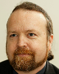
Octavo
Systems
 |
 Gene
Frantz – CTO, Octavo Systems. Gene
Frantz – CTO, Octavo Systems.
“Integration Beyond
System-on-Chip: The System-in-Package.”
Abstract: The semiconductor
industry has depended on Silicon Integration to meet the ever-demanding
needs of their customers. This has led to ever more complex System-on-Chip
(SoC) designs, integrating a wide variety of disparate functions. However,
as the demands of end systems have continued to increase and Silicon
processes continue to specialize the possibility of integrating everything
into a single die has become increasingly difficult, forcing SoC to really
be SSoC (Sub-System on Chip). If the semiconductor industry wants to
continue to integrate the features customers are demanding, a new solution
to future integration must be found. The new solution is System-in-Package.
This presentation will discuss the need for System-in-Package technology and
how it can work with SSoC to meet the future needs of customers.
Bio: Gene is one of the founders and the visionary behind Octavo Systems. He
currently serves as Chief Technology Officer. He is also a Professor in the
Practice at Rice University in the Electrical and Computer Engineering
Department. Previously, Gene was the Principal Technology Fellow at Texas
Instruments where he built a career finding new opportunities and building
new businesses to leverage TI’s DSP technology. Through this work he became
highly regarded in the industry as a leader in DSP technology. Gene holds 48
patents, has written over 100 papers/articles and presents at conferences
around the globe. He has a BSEE from the University of Central Florida, a
MSEE from Southern Methodist University, and a MBA from Texas Tech
University. He is also a Fellow of the IEEE.
|
|
|
|
LG Electronics Mobile Communications
Keynote
 |
 Dr.
Yasser Nafei, Senior Vice President LG Electronics Mobile Communications. Dr.
Yasser Nafei, Senior Vice President LG Electronics Mobile Communications.
“Accelerating the adoption of
5G: The journey towards a consumer centric vocabulary"
Abstract: TBD.
Bio: Yasser Nafei currently
serves a Senior Vice President and division head at LG Electronics. Dr.
Nafei joined LG in 2010 and currently oversees strategy, sales and business
development for mobile business unit. In his current role, he is responsible
for developing, communicating and executing LG strategy, business plans,
product and technology roadmaps and go to market activities. Throughout his
career, Dr. Nafei previously held senior management positions at Alcatel,
IBM, Motorola, Nortel and Tellabs. His global assignments include research &
development, technology strategy, mergers & acquisitions, sales & marketing
along with quality and service operations. Dr. Nafei holds a
Bachelor’s and a Masters’ degrees in Electrical Engineering from Ain Shams
University in Egypt, a Master of Science in Telecommunications from INRS
Canada, and a Ph.D. in Organization Development from Benedictine University
in the United States. He is the author of several business books including
“Corporate Dictatorship ISBN 978-0982328743 and Corporate Spring ISBN
978-0982328750. He is a published writer and lecturer in future technology
trends, consumer centric research, corporate governance, business turnaround
strategies, conflict management, customer advocacy and mergers &
acquisitions.
|
|
|
|
Lunch
|
Lunch |
|
|
|
UC Irvine
|
 Dr.
Fadi J Kurdahi, Center for Embedded & Cyber-physical Systems, University of
California, Irvine. Dr.
Fadi J Kurdahi, Center for Embedded & Cyber-physical Systems, University of
California, Irvine.
“Towards Self-Aware
Systems-on-Chip Through Intelligent Cross-Layer Coordination.”
Abstract: Although there is a
rich history of cross-layer design for embedded computing systems to achieve
desired QoS, we are facing ever more challenges from the intertwined goals
of energy- efficiency, thermal design constraints, as well as resilience to
errors emanating from the application, environment and hardware platforms.
We posit that next-generation computing platforms must necessarily deploy
intelligent cross-layer design achieved through self-awareness principles
inspired by biology and nature. Such an approach will move us from current
strategies (using limited cross-layer coordination) to a holistic
cross-layer strategy that enables intelligent cross-layer management
policies which can adaptively tune itself based on the current state of the
system. The talk will present design exemplars that embrace this intelligent
cross-layer approach, and highlight the role of self-awareness in achieving
dynamic adaptivity.
Bio: Fadi Kurdahi received his PhD from the University of Southern
California in 1987. Since then, he has been a faculty at the Department of
Electrical & Computer Engineering at UCI, where he conducts research in the
areas of Computer Aided Design and design methodology of large scale
systems. He serves as the Associate Dean for Graduate and Professional
Studies of the Henry Samueli School of Engineering, and the Director of the
Center for Embedded & Cyber-physical Systems (CECS), comprised of
world-class researchers in the general area of Embedded and Cyber-physical
Systems. He served on numerous editorial boards, and was program chair or
general chair on program committees of several workshops, symposia and
conferences in the area of CAD, VLSI, and system design. He received the
best paper awards for the IEEE Transactions on VLSI in 2002, ISQED in 2006
and ASP-DAC in 2016, and other distinguished paper awards at DAC, EuroDAC,
ASP- DAC and ISQED. He also received the Distinguished Alumnus award from
his Alma Mater, the American University of Beirut in 2008. He is a Fellow of
the IEEE and the AAAS.
|
|
|
|
UCLA
 |
Dr.
Boris Vaisband, UCLA Engineering Dept.
“Design of Ultra-Large
Wafer-Level Systems.”
Abstract: Silicon interconnect
fabric (Si-IF) is a compatible wafer-level platform to satisfy the needs of
heterogeneous ultra large scale systems (e.g., neuromorphic systems). Si-IF
provides an opportunity to reduce both, the distance between chips and the
vertical interconnect pitch. Bare (unpackaged) dies are placed directly on
the passive Si-IF platform that effectively replaces the printed circuit
board. The Si-IF supports integration of heterogeneous dies including III-V,
MEMS, and sensor dies. The dies are connected using fine pitch vertical
interconnects (pillars) designed directly on the Si-IF. The pitch of the
vertical pillars that are used to bond dies to the Si-IF is 2 to 10 μm, and
the minimal distance between adjacent dies on the Si-IF is approximately 50
to 100 μm. To enable the Si-IF as a practical platform for ultra large scale
heterogeneous integration, system-level issues, similar to a large system on
chip (SoC), must be addressed. A network on interconnect fabric (NoIF) is
proposed to support global communication (e.g., RF and optical
interconnects), power management (including multiple technologies and
voltage domains), synchronization, and to facilitate testing within the Si-IF.
The Si-IF is a passive platform; utility dies (UDs) serve, therefore, as
intelligent nodes within the NoIF. Various parameters must be considered
when designing the NoIF, including communication performance, power,
functionality, yield, and cost.
Bio: Boris Vaisband is currently a postdoctoral scholar at the University of
California, Los Angeles, working on wafer-level heterogeneous system
integration. He received a B.Sc. degree in Computer Engineering from the
Technion – Israel Institute of Technology, Haifa, Israel in 2011, and an
M.S. and Ph.D. degrees in Electrical Engineering from the University of
Rochester, Rochester, NY, in, respectively 2012 and 2017. Between 2008 and
2011, he held a hardware design position at Intel Corporation in Israel. In
the summer of 2013, he interned with the Optical and RF research group at
Cisco Systems Inc., San Jose, CA. In the summer of 2015, he interned with
the Power Design team at Google Inc., Mountain View, CA. His current
research interests include integration of heterogeneous systems, power
delivery, communication, thermal aware design and floorplanning, and noise
coupling for high performance computing, IoT, and bio-compatible systems.
|
|
|
|
ANSYS,
Inc.
 |
 Dr.
Norman Chang co-Founded Apache Design Solutions in 2001, and currently
serves as Chief Technologist at Semiconductor BU, ANSYS, Inc. Dr.
Norman Chang co-Founded Apache Design Solutions in 2001, and currently
serves as Chief Technologist at Semiconductor BU, ANSYS, Inc.
“Emerging ADAS Thermal
Reliability needs and Solutions."
Abstract: Advanced Driver
Assistance Systems (ADAS) used for pedestrian detection, parking assist,
night vision, blind spot monitoring, collision avoidance and other such
capabilities have significantly enhanced car safety and reduced the risk of
dangerous accidents. These technologies are enabled through sensors,
cameras, advanced processors and intelligent software for continuously
sensing the environment, gathering, and processing the data to make
meaningful decisions in real time. They are further evolving to create a
network of intelligent systems using vehicle-to-infrastructure (V2I) and
vehicle-to-vehicle (V2V) communications, thus paving the way for autonomous
driving. To support these advanced technologies, automotive electronics
require to be overhauled to enable Machine Learning and particularly Deep
Learning capabilities to transform the typical car into a smart system on
wheels. Thermal reliability becomes very critical for these high-power,
intelligent electronics systems since it needs to last more than 10 years
under often hostile thermal environments – temperature under the hood of the
car can go as high as 135°C to 150°C. This talk presents an innovative
multi-physics solution for thermal, thermal-aware EM, and thermal-induced
stress analysis of a Chip-Package-System realized in 3DIC, an example of
which is an AI system used in ADAS.
Bio: Norman Chang co-founded Apache Design Solutions in February 2001 and
currently serves as Chief Technologist at Semiconductor BU, ANSYS, Inc. He
is also currently leading the effort of applying ML/DL at ANSYS. Prior to
Apache, Dr. Chang lead a group at Palo Alto HP Labs, focused on interconnect
related signal/power integrity issues and contributing to the HP-Intel IA64
micro-processor design. Dr. Chang received his BS, MS, and Ph.D. in
Electrical Engineering and Computer Sciences from University of California,
Berkeley. He holds thirteen patents and has authored over 50 technical
papers. He also co-authored the popular book, "Interconnect Analysis and
Synthesis", published by John Wiley & Sons, 2000. He is currently in the
committee for ESDA-EDA and SI2 Open3D TAB.
|
|
|
|
HPE

 |
Michael
Krause, VP and Fellow Engineer at HPE.
“Next-Generation Interface
- Gen-Z.”
Abstract: The public release
of the Gen-Z Core Specification 1.0 allows silicon providers and IP
developers to start working on products based on this exciting new
interface. Gen-Z is the right way to address the worldwide explosion of data
(180ZB annually by 2025) and the need for a high throughput, low-latency,
scalable, memory-centric fabric. Gen-Z responds to the rapid rise in the
number of extremely fast devices and enables a memory-centric architecture
with full composability. It simplifies memory-to-memory transfers and
eliminates the need for side channels and DMA, thus avoiding
behind-the-curtain operations that are difficult to understand, evaluate,
debug, or update. Gen-Z is designed with security as a key tenet and
contains embedded access and security rights. Future versions of Gen-Z will
meet the needs of emerging applications such as artificial intelligence,
cognitive computing, real-time data analysis, the Edge, and autonomous
systems.
Bio: Michael Krause supports the HP Servers area of the Enterprise Group,
where he is focused on developing new computer and memory architectures and
developing HP strategies on a range of technologies. In a career spanning
nearly three decades at HP, Krause has worked in a variety of positions
developing deep expertise in I/O, OS, storage, memory, virtualization, and
high speed
network and fabric architectures. He also chairs the HP Servers Technical
Career Path Promotion Board and is active in mentoring and developing HP’s
technical community. Widely admired as an inventor, Krause has co-developed
and led HP in the creation of numerous technologies including PCI Express,
InfiniBand, single and multi-Root I/O Virtualization, ATS, RDMA, M-PCIe, HMC,
and Ethernet DCB / EVB. He has also been an active contributor to key
industry associations, including the PCI-SIG, IETF, IEEE, DMTF, InfiniBand
TA, and USB-IF. Krause received his B.S. and M.S. in computer engineering
from San Jose State University
|
|
|
|
Intrinsic ID

|
 Dr.
Pim Tuyls, Founder and Chief Executive Officer, Intrinsic ID. Dr.
Pim Tuyls, Founder and Chief Executive Officer, Intrinsic ID.
"Securing the IoT via a
Software-Delivered Hardware Root of Trust"
Abstract: As concern for
securing the Internet of Things continues to escalate, so does the need for
a reliable root of trust to establish a unique, immutable and unclonable
identity for any connected device. A root of trust establishes an anchor
point for security, and drives critical system security functions such as
device-to-cloud authentication, secure device life cycle, encryption and IP
protection. Today's market and economic dynamics mandate increased
flexibility in deploying IoT security, flexibility that is best achieved by
delivering a root of trust via software. This presentation will describe how
a software-deployed root of trust offers technology and economic advantages
previously unavailable to the IoT.
Bio: Pim Tuyls is CEO of Intrinsic ID, a company specializing in IoT
security technology. Before founding Intrinsic ID in 2008 he was at Philips
Research, where he was Principal Scientist and managed the cryptography
cluster. While there he initiated the work on Physical Unclonable Functions
(PUFs), which forms the basis of Intrinsic ID’s silicon fingerprinting
technology. Tuyls has a Ph.D. in mathematical physics from Leuven
University, holds more than 50 patents and is widely acknowledged for his
work in the field of security for embedded applications.
|
|
|
|
Synopsys,
Inc.
 |
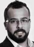 Mina
J Hanna, Sr. Application Consultant, Static Timing Analysis, PrimeTime
Suite, Synopsys, Inc. Mina
J Hanna, Sr. Application Consultant, Static Timing Analysis, PrimeTime
Suite, Synopsys, Inc.
Chair, IEEE-USA AI & AS Policy Committee, Vice chair, IEEE-USA R&D Policy
Committee, Co- Chair, IEEE-SA Global Initiative on Ethics of A/I Systems,
Policy Committee
“The Policy and Law
Background to Net Neutrality, and the recent FCC Ruling to upend it."
Abstract: The debate over net
neutrality has been contentious since the early days of the Internet. It has
repeatedly been challenged in court by Internet service providers (ISPs) for
years, culminating in the latest decision by the Federal Communications
Commission (FCC) to upend the 2015 net neutrality ruling. Critics see this
decision as a threat to Internet consumer freedoms, economic competition
(imposing a significant market disadvantage on small businesses), and even
the progress of scientific research and knowledge discovery. Seeing how
important the Internet is to the advancement of innovation, development of
human capital, and economic growth, it is imperative for technologists,
researchers, and innovators to take heed of the policy debate and the latest
developments. On 18 May, 2017, the FCC voted to put forth the Restoring
Internet Freedom Notice of Proposed Rulemaking (NPRM), seeking comments on a
proposal to roll back the 2015 net neutrality regulations. In 2015, the
Obama administration passed a rule to classify the Internet as a public
utility under Title II of the 1934 Communications Act. The rule prohibits
ISPs from preferentially allocating bandwidth for affiliated content,
throttling bandwidth, or implementing preferential price structures for
their customers. Several months later, on December 14, the FCC moved forward
with their decision to repeal the rule after a 3–2 party-line vote.
Bio: Mina J. Hanna is a senior software consultant at Synopsys, Inc., the
current Chair of the IEEE-USA Artificial Intelligence and Autonomous Systems
Policy Committee, the current Vice Chair of the IEEE-USA Research and
Development Policy Committee and the Chair of the IEEE Central Texas Section
Government Relations, Policy and Regulations Committee. He serves as Editor
of the Science Policy Column and a member of the editorial board of IEEE
Computer magazine. He is also a member of the IEEE Global Initiative for
Ethical Considerations in Artificial Intelligence and Autonomous Systems,
the IEEE Computational Intelligence Society, the IEEE Society on Social
Implications of Technology and IEEE TechEthics. Prior to joining Synopsys,
he worked for 6 years at Intel in the Platform Engineering Group on the
Intel Atom Processors and SOCs, having contributed to 10+ tapeouts. Mina
received an MSc in Electrical Engineering from Stanford University, and a
BSc in Electrical Engineering from the University of Texas-Austin.
Professor Scott Jordan, from University of California, Irvine is
substituting for Mina Hanna.
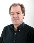 Scott
Jordan, Professor of Computer Science at the University of California,
Irvine. Scott
Jordan, Professor of Computer Science at the University of California,
Irvine.
Scott Jordan is a Professor of
Computer Science at the University of California, Irvine. His research has
focused on Internet quality of service issues, including traffic management
and resource allocation, in both wired and wireless networks. His current
research interests are Internet policy issues, including net neutrality,
data caps, and device attachment. Scott received the Ph.D. degree in
Electrical Engineering & Computer Science from the University of California,
Berkeley. In 2006, he served as an IEEE Congressional Fellow, working in the
United States Senate on communications policy issues. In 2014-2016, Scott
served as the Chief Technologist at the Federal Communications Commission,
advising on technological issues across the Commission.
|
|
|
|
Panel
"FREE"
|
Panel:
“Are you ready for the Blockchain of Things? Blockchain & Semiconductors
Economy – Hypes, Realities, and Opportunities."
Abstract: Blockchain is the technology at the heart of bitcoin and other
virtual currencies. It is an open and distributed ledger that can record
transactions between two parties efficiently and in a verifiable and
permanent way. What makes this system theoretically tamperproof is two
things: a cryptographic fingerprint unique to each block, and a “consensus
protocol,” the process by which the nodes in the network agree on a shared
history. Many industry analysts believe that Blockchain technology is the
solution for many of the security, privacy and reliability concerns in the
Internet of Things (IoT). The billions of smart devices coming to the IoT
could transform homes, cities and lives. But they also could create a
serious security headache. The combination of artificial intelligence, IoT
and Blockchain will bring multiple benefits across multiple industries,
leading to a whole host of IoT applications that we haven’t yet considered.
With billions of connected devices filling our homes, workplaces and cities,
security of data must keep pace. Could blockchain-based solutions offer a
viable alternative to current methods? In this panel, we will discuss hypes,
realities, and opportunities in Blockchain of Things and much more.
Moderator: Farhad Mafie, SoC Conference Chairman.
Panelists:
Panelists:
1. Dr. Bhaskar Krishnamachari, Professor of Electrical Engineering &
Computer Science; Director of Center for Cyber-Physical Systems and the
Internet of Things, USC Viterbi School of Engineering.
2. Erik Saberski, Data Scientist, XYO Network.
3. Ben Taylor, CEO, LedgerDomain.
4. Raghu Bala, CEO, NetObjex.
5. Eman Hashem Safadi, Blockchain Strategy Consultant, CoFounder LA
Blockchain Lab, Blockchain Strategy Consultant, ObEN, Inc.
6. Stephan Wullschleger, CTO, PBV Kaufmann.
This
Panel Is Open To Everyone . . .
Register Online for FREE Panel Pass
|
|
|
|
Savant
Company Inc.
SoC Conference


 |
Farhad
Mafie, SoC Conference Chairman.
Moderator
Farhad Mafie, President and
CEO of Savant Company Inc., that provides marketing and business development
services to high-tech startups and mid-size companies on a worldwide basis.
He has over 25 years of experience in high-tech industries including
semiconductor and computer businesses; additionally, he has more than 15
years of university-level teaching experience.
In 2003, Farhad designed and
developed the annual Internationals System-on-Chip (SoC) Conference,
Exhibits, and Workshops. As the SoC Conference Chairman, he drives the
Conference leading-edge annual program.
As Chief Marketing Officer (CMO)
for a Switzerland startup, Farhad is driving an innovative mobile payment
system based on selected concepts that are very similar to Blockchain.
For almost six years at
Microsemi Corporation, as Vice President of Worldwide Product Marketing and
Corporate Communications teams (in US, EU, India, and China), Farhad
developed and managed the entire Microsemi’s worldwide outbound and inbound
marketing strategies and programs; and worked directly with executive team
on M&A projects and successfully integrating over 18 acquired companies.
Farhad is also the former Vice
President of Marketing/Business Development and Technical Sales Engineering
at Toshiba America Electronic Components, Inc. He was responsible for
marketing the entire Toshiba standard ICs in North America, as well as
engineering development for Toshiba's Embedded and Digital Consumer products
& solutions based on ASSP and SoC Models.
Farhad has worked at Lucent Technologies on marketing communications ICs,
Toshiba Information Systems on product definition for Toshiba's notebooks
PCs and handheld products, Unisys on designing new processors and computer
systems, Ocean Scientific on designing medical instrumentations, and MSI
Data on designing data collection products. He has a Master of Science and a
Bachelor of Science degree in Electronic Engineering from California State
University, Fullerton.
He is an author and a
translator. In 2003, he published the biography of Iranian poet and Nobel
nominee who lived in exile, Nader Naderpour (1929-2000), Iranian Poet,
Thinker, Patriot. Farhad is also Editor-in-Chief for the CRC Press SoC
Design and Technologies Book Series, which includes (1) Low-Power NoC for
High-Performance SoC Design and (2) Design of Cost-Efficient Interconnect
Processing Units. Farhad is an active member of IEEE, and he is the chair of
IEEE Orange County Solid-State Circuits Society (SSCS), as well as IEEE
Orange County Entrepreneurs' Network (OCEN). He is also a member of two UCI
Advisory Committees: Communication System Engineering and Embedded System
Engineering Certificate Programs.
|
|
|
|
ObEN, Inc.
Panelist
|

Eman Safadi – COO, LA
Blockchain Lab & Principal, EHS Consulting.
Panelist
Bio: Eman is a strategy
consultant and general manager who helps organizations identify and
implement key technologies that can fundamentally change their business,
most recently focusing on blockchain, tokenomics, and use cases across the
healthcare vertical. She is also the COO of the LA Blockchain Lab, a
collaboration of UCLA, UCI, USC, Caltech, the City of LA, enterprises,
startups, and nonprofits working to build the blockchain ecosystem in
Southern CA. Prior to moving to LA, she led key technology initiatives for
the Dept of Education to overhaul and modernize the FAFSA process and its
underlying solutions and technologies. She spent a year in Jordan as Chief
of Staff for HM Queen Rania where she strategically reorganized and oversaw
all local and international operations. Previously, Eman cofounded Xypnos, a
developer of embedded software for IoT devices and Ultiverse, a
cross-platform messaging venture. She spun off and ran WorldCare
Technologies, which operates the largest telemedicine network
internationally and spent time at the World Bank, McKinsey, and Verizon
Broadband Services. She holds an MS in computer science from MIT and an MBA
from Harvard Business School.
|
|
|
|
USC
Panelist
|
Dr.
Bhaskar Krishnamachari, Professor of Electrical Engineering & Computer
Science; Director of Center for Cyber-Physical Systems and the Internet of
Things, USC Viterbi School of Engineering.
Panelist
Bio: TBA. |
|
|
|
LedgerDomain
Panelist
|
 Ben
Taylor, CEO, LedgerDomain. Ben
Taylor, CEO, LedgerDomain.
Panelist
Bio: TBA. |
|
|
|
NetObjex
Panelist
|
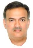 Raghu
Bala, CEO, NetObjex. Raghu
Bala, CEO, NetObjex.
Panelist
Bio: TBA. |
|
|
|
XYO Network
Panelist
|
 Erik
Saberski, Data Scientist, XYO Network. Erik
Saberski, Data Scientist, XYO Network.
Panelist
Bio: In 2018, Erik joined the
XYO team as the lead mathematician and data scientist while pursuing his PhD
in Biological Oceanography studying nonlinear dynamics, complexity theory,
and data-driven theory at the Scripps Institution of Oceanography (SIO). He
is fascinated by variable interactions within complex systems and uses
dynamic modeling techniques to understand the casualties in blockchain
markets, ecological systems, and even locations of objects. |
|
|
|
PBV
Panelist
|
Stephan
Wullschleger, CTO, PBV Kaufmann.
Panelist
Bio: TBA. |
|
|
|
|
Open To Everyone
Reception & Networking
|
|
|
|
|
16th International SoC
Conference Closed.
|
|
|
|
|
|
|
* * * * * * *
* SoC Conference Program is
subject to change. Savant Company Inc, SoC Conference Organizing
Committee, and Technical Advisory Board, reserve the rights to revise or modify
the SoC Conference agenda at its sole discretion.
Back To The Main SoC
Conference Page
Copyright © 2003-2018 by Savant Company Inc. All
Worldwide Rights Reserved. | |
|