|
| |
|
SoC Conference Presenters'
Bios & Abstracts
15h International System-on-Chip
(SoC)
Conference, Exhibit & Workshops
The Theme for This
Year’s Conference Is “Secure and Intelligence Silicon Systems for
Emerging Applications."
|
 |
|
To present and/or exhibit at this
highly-targeted International System-on-Chip (SoC) Conference, please contact:
949-981-1837 or SoC.Conf.Update@Gmail.com
|
|
|
Click Here To
Download The UCI Campus Map
Directions &
Parking for Calit2 Building at the University of California, Irvine (UCI)
Platinum Sponsors
Click Here To
Download The UCI Campus Map
Directions &
Parking for Calit2 Building at the University of California, Irvine (UCI)
|
|
|
|
|
|
|
|
Day
One Wednesday October 19, 2016
SoC Conference Program Agenda* |
|
|
|
Savant
Company Inc.
 |
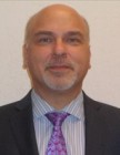
 Farhad
Mafie, SoC Conference Chairman,
IEEE OC SSCS & OCEN Chairs. Farhad
Mafie, SoC Conference Chairman,
IEEE OC SSCS & OCEN Chairs.
Welcome and Opening Remarks, Technology/Market Trends.
Farhad Mafie is SoC Conference
Chairman. He has over
20 years of experience in semiconductor and computer businesses and more
than 10 years of university-level teaching experience. He is the former Vice
President of Marketing and Engineering at Toshiba Semiconductor. He has also
worked in strategic marketing, project and design engineering at Lucent
Technologies, Unisys, and MSI Data. Farhad has a Master of Science and a
Bachelor of Science degree in Electronic Engineering from California State
University, Fullerton. He is an author and a translator, and his articles
have been published in a variety of journals and Web-based magazines on
technology and political affairs. In 2003, he published the biography of
Iranian poet and Nobel nominee who lived in exile, Nader Naderpour
(1929-2000), Iranian Poet, Thinker, Patriot. Farhad is also Editor-in-Chief
for the CRC Press SoC Design and Technologies Book Series, which includes
(1) Low-Power NoC for High-Performance SoC Design and (2) Design of
Cost-Efficient Interconnect Processing Units. Farhad is an active member of
IEEE, and he is the chair of IEEE Orange County Solid-State Circuits Society
(SSCS), as well as IEEE Orange County Entrepreneurs' Network (OCEN). He is
also a member of two UCI Advisory Committees: Communication System
Engineering and Embedded System Engineering Certificate Programs.
|
|
|
|
4DS Memory Limited.
 |
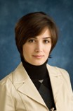
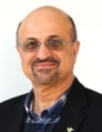
 Dr.
Seshubabu Desu, Chief Technical Officer, 4DS Memory Limited. Dr.
Seshubabu Desu, Chief Technical Officer, 4DS Memory Limited.
"Emerging Memories: Challenges and opportunities"
Abstract: This presentation
will focus on emerging memories in terms of their advantages and challenges
with respect to cost, scalability, density and performance. The metrics that
are needed for predicting the potential success of these technologies will
be analyzed. The physical picture behind the interdependence of endurance,
retention, and bit error rates will be emphasized so that the performance
optimization could be accomplished. The unique characteristics of these
emerging memories for embedded applications as well as IOT, mobile and SCM
applications will also be discussed.
Bio:
Dr Seshubabu Desu is a highly regarded global subject matter expert in thin
films, semi processing and non-volatile memories. He is CTO at 4DS Memory
Limited that is pioneering non-filamentary resistive random access memory (ReRAM)
for next generation gigabyte silicon storage in mobile and cloud. Dr. Desu
currently leads the non-volatile memory technology and product development
for 4DS. Prior to this, he was Dean of SUNY Binghamton’s Watson School of
Engineering, Head of the Electrical and Computer Engineering Department at
University of Massachusetts Amherst, and a professor at Virginia Tech
Blacksburg. He holds 30 US patents, has written over 240 refereed technical
articles and is a Highly Cited Researcher. Dr. Desu has co-edited six books
and supervised over 35 MS and PhD theses. He is a Fellow of both IEEE and
the American Ceramic Society. His previous experience includes being a Group
Leader at GE and a Senior Member of Technical Staff at Bell Laboratories. He
holds a PhD in Materials Science and Engineering from the University of
Illinois at Urbana-Champaign.
|
|
|
|
SK Hynix

|
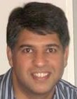
 Kevin
Tran is a Sr. Manager of Technical Marketing at SK Hynix and Vis Valluri is
the Director for Market Intelligence at SK Hynix Kevin
Tran is a Sr. Manager of Technical Marketing at SK Hynix and Vis Valluri is
the Director for Market Intelligence at SK Hynix
"Memory technology targeting
smart applications enabled by 5G networks"
Abstract: While the scope of a 5G network is being finalized, one
thing is clear – 5G is going to have a significant change in the way it
impacts industries and business models. Very few could envision the
proliferation of the smartphones and its impact on the transportation
industry, yet we expect even more industry segments/business models to be
impacted with the deployment of 5G. As an example, in addition to existing
revenue streams, we believe markets/industries will move towards a services
driven revenue model – enabled by the increased data capture and ability to
provide data analytics and offer compelling value based solutions. The talk
will cover key markets that will be impacted by 5G like Automotive,
Augmented-Reality/Virtual Reality (AR/VR), Artificial Intelligence (AI) and
the IoT segments and the opportunities for SoC/IC growth in these markets.
SoCs continue to evolve to meet the changing application requirements and
technical specifications of next generation system architectures. The memory
subsystem is a key area which can enable higher effective performance of
next generation SoCs. This talk will look at how next generation memory
devices address the key requirements of SoC targeting automotive, AR/VR, AI
and IoT applications. Bandwidth intensive system such as autonomous driving
vehicle will require hundreds of gigabytes of data per second while low
power and small form factor are critical for IoT and AR/VR applications.
Computing platforms targeting Artificial Intelligence will be massively
parallel and require memory subsystem that can deliver high bandwidth and
high capacity. We will review the key characteristics of next generation low
power DDR, graphics and memory devices leveraging Through Silicon Via (TSV)
to deliver high bandwidth, high capacity, low power and small form factors.
This new group of memory technologies will enable more intelligent systems
leveraging 5G networks.
Bio: Vis Valluri is the Director for Market Intelligence at SK Hynix focused
on the DRAM and NAND markets. Vis has over 20 years of experience in the
semiconductor industry and has worked in various functions ranging from
manufacturing, marketing, and more recently in corporate strategy. Vis was
previously in the Corp Strategy group at SanDisk for close to 4 years,
focused on the NAND market, leading market research for the retail and
mobile segments. Before joining SanDisk, he spent 5 years doing equity
research focused on semis, semicap and solar at Credit Suisse and Morgan
Stanley. Prior to his Wall Street career, Vis worked in
manufacturing/operations at AMD and marketing at KLA Tencor. He has a MBA
degree from Cornell University, MS in Mechanical Engineering from the State
University of New York, and a BS degree from the Indian Institute of
Technology.
Kevin Tran is a Sr. Manager of Technical Marketing at SK Hynix where his
primary focus is on advanced memory solutions for high performance
applications including networking, high performance compute and automotive.
He is also the HBM Program Manager for SK Hynix America and has been
developing the ecosystem to enable HBM in 2.5D integration. Kevin has over
14 years of experience in applications engineering and technical marketing
in the semiconductor industry. He has worked for Atmel, Micron and Nanya
prior to joining SK Hynix.
|
|
|
|
Western Digital Corporation

|
 Dr.
Luis Vitorio Cargnini, Research Technologist Engineer, Western Digital
Corporation Dr.
Luis Vitorio Cargnini, Research Technologist Engineer, Western Digital
Corporation
“NoC as Interconnect Fabric for Emerging Non-Volatile Memories.“
Abstract: Memory chips have been designed in a stereotypical fashion
for decades. Arrays and sub-arrays of memory elements are organized in such
way providing spaces across subarrays, to allow the so-called “H-tree”
routing structures, with a "sea-of-metal-tracks" carrying the bits across
the chip to the digital interface. This scheme is running into scalability
limits, with over two thirds of the chip area accommodating this
sea-of-metal in some recent designs. These scalability problems are further
exacerbated with emerging non-volatile memories, such as Magnetic RAM (MRAM),
Phase Change Memory (PCM) and Resistive-RAM (ReRAM), that scale to even
smaller memory cells. We explored a new memory bank architecture
organization, one that keeps the traditional memory cell sub-array, but
replaces the sea-of-metal routing with a Network-on-Chip. In this
presentation we will argue that this design methodology provides better
decoupling of data from communication, and is more amenable to innovation in
the inevitable evolution of the interface as well as to more rapid
deployment of new types of memory. Further, this architecture creates
opportunities for more radical innovation in the CPU and SoC architectures,
such as the hardware acceleration of coherence to even larger pools of
globally shared memory or extending the memory hierarchy to a distributed
coherence over fabric. Allowing SoC designers to explore new levels of
performance with better controlled latency and predictable scalability.
Bio: Dr. Cargnini is currently a Research Technologist Engineer at the
Western Digital Corporation Research Center, in San Jose, California,
formerly known as HGST Research Center. He joined the Company in 2014 in the
Storage Architecture group under Director Dr. Zvonimir Bandic and group
Manager Dr. Dejan Vucinic. Meanwhile he has been working in characterizing
MRAM and new emerging NVM memories, researching new Integrated Circuits
designs to allow WDC to leverage emerging NVMs technologies with minimum
impacts to a system performance. Also, his group is currently investigating
and exploring ideas on how to extend the memory coherence all the way to the
storage devices and how to aggregate higher processing functionality into a
storage device, as well as new I/O architecture and organizations
technologies from the IC level all the way to the system level. Previously
to join WDC, he was a Research Engineer and obtained his Ph.D at the
Laboratoire d’Informatique, de Robotique et de Microélectronique de
Montpellier (LIRMM) at the Université de Montpellier in France, under the
supervision of professor Dr. Lionel Torres, and his thesis was entitled
“MRAM APPLIED TO EMBEDDED PROCESSORS ARCHITECTURE AND MEMORY HIERARCHY”.
|
|
|
|
Morning Break |
Morning Break |
|
|
|
Microsemi

|
 Dr.
Rino Micheloni is Engineering Fellow at Microsemi Corporation. Dr.
Rino Micheloni is Engineering Fellow at Microsemi Corporation.
“Impact of 3D Flash Memories on SSD’s Controller Design.“
Abstract: Flash memory has been a disruptive technology from its
inception in the early '90s and innovation is still ongoing after more than
25 years. Thanks to their storage density, NAND Flash memories have changed
our lives: USB keys have replaced floppy-disks and Flash Cards (SD, eMMC)
record our pictures and movies instead of analog films. In the last 4-5
years Solid State Drives (SSDs) have emerged as the new killer applications
for Flash: first in the consumer space (smartphones and tablets) but now
expanding to enterprise applications as well. Indeed, being extremely
demanding in terms of storage capacity, SSDs fueled a new revolutionary wave
of innovations: 3D Flash memories. Today “3D” is a common buzzword but in
this specific case it means that multiple layers (up to 64, as we speak) of
memory cells are manufactured within the same piece of silicon. In this
paper we review the evolutionary path from planar to 3-dimensional NAND
Flash memories, and its impact on the design of the Flash Controller located
inside a Solid State Drive, with specific reference to enterprise
applications, which are the most demanding in terms of performances and
reliability.
Bio: Dr. Rino Micheloni is Engineering Fellow at Microsemi Corporation where
he currently runs the Non-Volatile Memory Lab in Milan, with special focus
on NAND Flash. Prior to joining Microsemi, he was Fellow at PMC-Sierra,
working on NAND Flash characterization, LDPC, and NAND Signal Processing as
part of the team developing Flash controllers for PCIe SSDs. Before that, he
was with IDT (Integrated Device Technology) as Lead Flash Technologist,
driving the architecture and design of the BCH engine in the world’s 1st
PCIe NVMe SSD controller. Early in his career, he led NAND design teams at
STMicroelectronics, Hynix, Infineon, and Qimonda; during this time, he
developed the industry’s first MLC NOR device with embedded ECC technology
and the industry’s first MLC NAND with embedded BCH. Rino is IEEE Senior
Member, he has co-authored more than 50 publications, and he holds 242
patents worldwide (including 120 US patents). He received the
STMicroelectronics Exceptional Patent Award in 2003 and 2004, and the
Qimonda IP Award in 2007.
Rino has published the following books with Springer: 3D Flash Memories
(2016), Inside Solid State Drives (2013), Inside NAND Flash Memories (2010),
Error Correction Codes for Non-Volatile Memories (2008), Memories in
Wireless Systems (2008), and VLSI-Design of Non-Volatile Memories (2005).
|
|
|
|
IBM
 |
 Dr.
Daniel Worledge, Distinguished Research Staff Member, Senior Manager,
MRAM, IBM. Dr.
Daniel Worledge, Distinguished Research Staff Member, Senior Manager,
MRAM, IBM.
"Spin Torque MRAM."
Abstract: Spin-Transfer-Torque Magnetic Random Access Memory (MRAM)
possesses a unique combination of high speed, high endurance,
non-volatility, and small cell size. Among the emerging new memory
technologies, including phase change memory, resistive random access memory,
and conductive bridging random access memory, Spin Torque MRAM is the only
candidate with the potential for unlimited endurance, since no atoms are
moved during writing. This makes it the only potential candidate for use as
a non-volatile working memory. Write current largely determines the cost of
Spin Torque MRAM, since the transistor and hence cell area must be sized
large enough to source the write current. This talk will give a brief
overview of Spin Torque MRAM, including potential applications and materials
challenges. I will then review the discovery of interface perpendicular
anisotropy in the Ta|CoFeB|MgO system at IBM and the subsequent
perpendicular magnetic tunnel junctions which were developed using it,
including demonstration of reliable, high speed spin-torque writing, and
results on scaling down to 20 nm. Recent experimental results showing low
switching current with 10 ns pulses and theoretical predictions for further
lowering the switching current will also be shown.
Bio: Dr.Daniel C. Worledge IBM Research Division, Almaden Research Center
Dr. Worledge received a BA with a double major in Physics and Applied
Mathematics from UC Berkeley in 1995. He then received a PhD in Applied
Physics from Stanford University in 2000, with a thesis on spin-polarized
tunneling in oxide ferromagnets. After joining the Physical Sciences
Department at the IBM T. J. Watson Research Center as a Post-doc in 2000, he
became a Research Staff Member in 2001, developing fast turn-around
measurement methods for magnetic tunnel junctions, including
Current-in-Plane Tunneling. In 2003, Dr. Worledge became the manager of the
MRAM Materials and Devices group, and in 2013 he became Senior Manager of
MRAM. He has worked on developing Toggle and then Spin Torque MRAM,
including developing new perpendicular magnetic materials. His current
research interests include magnetic devices and their behavior at small
dimensions, and new magnetic devices for logic applications.
|
|
|
|
Lunch |
Lunch |
|
|
|
Microsemi
|
 Ted
Marena, Director FPGA SOC Marketing, Microsemi Ted
Marena, Director FPGA SOC Marketing, Microsemi
“Microsemi highly-integrated and lowest power FPGAs enable unique camera
applications“
Abstract: Because Microsemi FPGAs offer more resources in lower density
FPGAs at up to 50% less power, engineers are able to create numerous unique
camera designs. This presentation will discuss various image sensor
interfaces and explain how Microsemi can support these. Typical image
processing functions that can be implemented, designs which benefit by using
Microsemi FPGAs and block diagram details of unique camera based products
will be shown.
Bio: Ted Marena is the director of FPGA SOC marketing at Microsemi. He has
over 20 years’ experience in FPGAs. He was awarded Innovator of the Year in
February 2014 when he worked for Lattice Semiconductor. Marena has defined,
created and executed unique marketing platform solutions for vertical
markets including consumer, wireless small cells, industrial, cameras,
displays and automotive applications. Marena started working as a design
engineer, field application engineer and a sales manager before he moved to
marketing. His understanding of the complete electronics design cycle has
earned him a reputation as an expert marketer in the semiconductor industry.
Marena holds a Bachelor of Science in electrical engineering Magna Cum Laude
from the University of Connecticut and a MBA from Bentley College’s Elkin B.
McCallum Graduate School of Business.
|
|
|
|
Microsemi
Keynote
|
 Jim
Aralis, Chief Technology Officer (CTO), and Vice President of R&D, Microsemi
Corporation. Jim
Aralis, Chief Technology Officer (CTO), and Vice President of R&D, Microsemi
Corporation.
Keynote:
“What does a SoC look like in 2025? Who, what and Why”
Abstract: The talk will
focus on changes in technology, applications, and economics of the SoC
ecosystem, and what it will likely mean for the realization of these devices
in the next decade. It will examine the way process technology, packaging
technology, design abstraction, and other such factors of true
differentiation will push these core devices. These observations are
intended to provide insights into where to position your company and career
for the coming decade.
Bio: Jim Aralis has served as
chief technology officer and vice president of R&D for Microsemi since
January 2007. He has more than 30 years experience in developing custom
analog device and process technologies, analog and mixed-signal ICs and
systems, and CAD systems. Jim played a key role in transitioning Microsemi to a virtually fabless
model, supporting multiple process technologies including, high voltage and
high power BCD/CMOS, high power high integration CMOS, GaAs, SiGe, IPD, RF
CMOS SoI, GaN, SiC, and several high-density packaging technologies.
From 2000 to 2007, Jim established and served as senior design director of
Maxim Integrated Product’s engineering center in Irvine, Calif. Before that,
he spent 7 years with Texas Instruments/ Silicon Systems as mixed-signal
design head and senior principal engineer. Additional experience includes 11
years with Hughes Aircraft Company in positions of increasing responsibility
including senior scientist. Jim earned a bachelor of science degree in
Math Applied Science and Physics and a master of science in electrical
engineering from UCLA. He holds 9 patents for circuit and system design.
|
|
|
|
University
of Michigan

|
 Dr.
Mina Rais-Zadeh, Associate Professor at University of Michigan, EECS
Department. Visiting Professor, Advanced Detectors, Systems & Nanoscience,
NASA JPL. Dr.
Mina Rais-Zadeh, Associate Professor at University of Michigan, EECS
Department. Visiting Professor, Advanced Detectors, Systems & Nanoscience,
NASA JPL.
“Reconfigurable front-end components for smart radio applications.“
Abstract: Currently, most electronic circuits are targeted for a
specific application and their functionality is fixed. There is a great
demand for smart electronics, where the system response can change in
different conditions. To develop such a system, in addition to sensor
integration for situation awareness, it is essential to develop adaptable
hardware. Examples of this are available mobile handsets, which can select
specific frequency bands. With advances in telecommunications, more and more
services rely on high data rate spectrum access, but the radio spectrum has
become overly crowded. Using reconfigurable or so called smart radios, one
can mitigate the problems associated with the limited spectrum availability
by tuning to the frequency band that is least heavily used at any given
time. To address this need, we are developing required hardware elements of
tunable radios. This talk covers a number of technologies developed for
smart radio applications including new switch structures using a
phase-change material, germanium telluride. Such switches are as small as
their semiconductor counterparts and can be integrated on silicon for
increased versatility but offer significantly lower loss and higher
isolation at the off state. The talk also describes how reconfigurable
radios can result in reduce entry costs in wireless phones.
Bio: Dr. Mina Rais-Zadeh received the B.S. degree in electrical engineering
from Sharif University of Technology and M.S. and Ph.D. degrees both in
Electrical and Computer Engineering from Georgia Institute of Technology in
2005 and 2008, respectively. From 2008 to 2009, she was a Postdoctoral
Research Fellow at Georgia Institute of Technology. In 2009, she joined the
University of Michigan, Ann Arbor, as an Assistant Professor of Electrical
Engineering and Computer Science (EECS). Since 2014, she has been an
Associate Professor in EECS with courtesy appointment in the Department of
Mechanical Engineering. In 2015, she is on sabbatical leave at NASA JPL. Dr.
Rais-Zadeh is the recipient of the NSF CAREER Award (2011), IEEE Electron
Device Society Early Career Award (2011), NASA Early Career Faculty Award
(2012), the Crosby Research Award from the University of Michigan (2013),
National Academy of Engineering Frontiers of Engineering (2013), ONR Young
Investigator Award (2014), and IEEE Sensors Council Early Career Technical
Achievement Award (2015). Together with her students, she received the best
poster award at the Transducers conference (2013), the best paper award at
the IEEE SiRF conference (2014), honorable mention at the IEEE IMS (2014),
and was the finalist in student paper competitions at the SiRF (2007) and
IMS (2011) conferences. She is an associate editor of IEEE Electron Device
Letters (EDL) and IEEE Journal of Microelectromechanical Systems (JMEMS) and
on editorial board of Nature Scientific Reports.
|
|
|
|
Xilinx

|
 Dan
Isaacs, Director of Connected Systems at Xilinx. Dan
Isaacs, Director of Connected Systems at Xilinx.
“Enhancing Intelligence at the Edge, Programmable SoCs for Accelerated Edge
Compute.“
Abstract: Complex algorithms, once requiring server‐class processing
to analyze massive amounts of sensor data, can now be accelerated in
programmable logic. This real-time processing performed "at the edge"
closest to the sensor input, reduces overhead and off chip communication, so
only the necessary information is transferred, enabling reduction of system
response time and improved operational efficiencies. Advantages to utilizing
advanced multiprocessor programmable SoCs in these systems compared to
conventional approaches will be compared and contrasted – where concerns
around performance, low latency, power, footprint, scalability, flexibility
and reliability are addressed in manners that today's devices with
comparable features cannot accomplish individually. The programmable
multiprocessor SoC presentation will include architectural details on
dedicated real time processing for low latency control / response while
simultaneously performing application processing for command and control.
Separation and isolation capabilities supported by the programmable SoC
architecture will be discussed in terms of hardware and software
capabilities. Industrial communication protocols with functionality, managed
by the processing system and / or the programmable logic will be presented.
Security and functional safety aspects, both integrated and third party
implementations, will be described in the context of Industrial IoT real
world applications.
Bio: Dan is Director of
Connected Systems at Xilinx. He is responsible for defining and executing
the ecosystem strategy for the Industrial IoT and is the representative to
the Industrial Internet Consortium. Dan has over 25 years of experience
working in mil/aero, automotive, and consumer based companies including
Hughes, Ford, NEC and LSI Logic. During his career, Dan has held positions
in software design, FPGA design engineer, systems engineer and system
verification, applications, other technical related management. He holds
degrees in Computer Engineering- EE from Cal State University, B.S.
Geophysics from ASU.
|
|
|
|
Afternoon Break |
Afternoon Break |
|
|
|
University of California,
Los Angeles.
Keynote

|
 Dr.
Subramanian S. Iyer, Distinguished Chancellor's Professor Dr.
Subramanian S. Iyer, Distinguished Chancellor's Professor
Charles P. Reames Endowed Chair, Electrical Engineering Department, Henry
Samueli School of Engineering and Applied Science, UCLA.
Abstract: Moore’s law
has so far relied on the aggressive scaling of CMOS silicon minimum features
of over 1000X for over four decades, and recently, on the adoption of
innovative features, such as Cu interconnects, low- dielectrics for
interconnects, strained channels, and high- materials for gate dielectrics,
resulting in a better power performance, cost per function, and density
every generation. This has spawned a vibrant system-on-chip (SoC) approach,
where progressively more function has been integrated on a single die. The
integration of multiple dies on packages and boards has, however, scaled
only modestly by a factor of three to five times. However, as SoC’s have
become more complex and bigger, the NRE and time to market have both
ballooned out of control leading to ever increasing consolidation. In this
presentation, we show that with the apparent slowing down of semiconductor
scaling and the advent of the Internet of Things, there is a focus on
heterogeneous integration and system-level scaling. Packaging is undergoing
a transformation that focuses on overall system performance and cost rather
than on individual components. We propose ways in which this transformation
can evolve to provide a significant value at the system level while
providing a significantly lower barrier to entry compared with a chip-based
SoC approach that is currently used. This transformation is already under
way with 3-D stacking of dies and will evolve to make heterogeneous
integration the backbone of a new SoC methodology.
Bio: Subramanian S. Iyer (Subu)
is Distinguished Chancellor’s Professor and holds the Charles P. Reames
Endowed Chair in the Electrical Engineering Department at the University of
California at Los Angeles and Director of the Center for Heterogeneous
Integration and Performance Scaling (CHIPS). He obtained his B.Tech. from
IIT-Bombay, and Ph.D. from UCLA and joined the IBM T.J. Watson Research
Center at Yorktown heights, NY and later moved to the IBM systems and
Technology Group at Hopewell Junction, NY where he was appointed IBM Fellow
and was till recently Director of the Systems Scaling Technology Department.
His key technical contributions have been the development of the world’s
first SiGe base HBT, Salicide, electrical Fuses, embedded DRAM and 45nm
technology used at IBM and IBM’s development partners to make the first
generation smartphone devices. He also was among the first to commercialize
bonded SOI for CMOS applications through a start-up called SiBond LLC. He
has published over 300 papers and holds over 70 patents. His current
technical interests and work lie in the area of advanced packaging and
three-dimensional integration for system-level scaling and new integration
and computing paradigms as well as the long-term semiconductor and packaging
roadmap for logic, memory and other devices including hardware security and
supply-chain integrity. He has received several outstanding technical
achievements and corporate awards at IBM. He is an IEEE Fellow and a
Distinguished Lecturer of the IEEE EDS as well as its treasurer. He is a
Distinguished Alumnus of IIT Bombay and received the IEEE Daniel Noble Medal
for emerging technologies in 2012. He also studies Sanskrit in his spare
time.
|
|
|
|
Panel
Fujitsu
Microsemi
IBM
UCI
NxGn Data,
Inc.
SoC
Conference
|
Panel:
“Memory
Trends and Innovations From Big Data to Mobile and Wearable Devices."
Moderator: Farhad Mafie, SoC Conference Chairman, IEEE OC SSCS &
OCEN Chairs.
Panelists:
1. Dr.
Daniel Worledge, Distinguished Research Staff Member, Senior Manager, MRAM.
IBM.
2. Dr. Rino Micheloni is Engineering Fellow at Microsemi Corporation.
3. Hitoshi Saito, Director, Emerging Memory Dept., System Memory Business
Div., FUJITSU SEMICONDUCTOR LIMITED.
4. Professor Nader Bagherzadeh, Electrical Engineering and Computer Science,
Donald Bren School of Information and Computer Science, UC Irvine.
5. Dr. Vladimir Alves, Co-founder, NxGn Data, Inc.
6. Jim Aralis, Chief Technology Officer (CTO), and Vice President of R&D,
Microsemi Corporation.
This
Panel Is Open To Everyone . . . Register Online for FREE Panel Pass
More
Updates Coming Soon . . .
Several
Opportunities to Win various Prizes During this Panel Discussion . . .
Don't
Miss Out!
|
|
|
|
Microsemi
|
Dr.
Rino Micheloni, Engineering Fellow at Microsemi Corporation.
Panelist
Bio: Dr. Rino Micheloni is Engineering Fellow at Microsemi Corporation where
he currently runs the Non-Volatile Memory Lab in Milan, with special focus
on NAND Flash. Prior to joining Microsemi, he was Fellow at PMC-Sierra,
working on NAND Flash characterization, LDPC, and NAND Signal Processing as
part of the team developing Flash controllers for PCIe SSDs. Before that, he
was with IDT (Integrated Device Technology) as Lead Flash Technologist,
driving the architecture and design of the BCH engine in the world’s 1st
PCIe NVMe SSD controller. Early in his career, he led NAND design teams at
STMicroelectronics, Hynix, Infineon, and Qimonda; during this time, he
developed the industry’s first MLC NOR device with embedded ECC technology
and the industry’s first MLC NAND with embedded BCH. Rino is IEEE Senior
Member, he has co-authored more than 50 publications, and he holds 242
patents worldwide (including 120 US patents). He received the
STMicroelectronics Exceptional Patent Award in 2003 and 2004, and the
Qimonda IP Award in 2007.
Rino has published the following books with Springer: 3D Flash Memories
(2016), Inside Solid State Drives (2013), Inside NAND Flash Memories (2010),
Error Correction Codes for Non-Volatile Memories (2008), Memories in
Wireless Systems (2008), and VLSI-Design of Non-Volatile Memories (2005).
|
|
|
|
IBM
|
Dr.
Daniel Worledge, Distinguished Research Staff Member, Senior Manager,
MRAM, IBM.
Panelist
Bio: Dr.Daniel C. Worledge IBM Research Division, Almaden Research Center
Dr. Worledge received a BA with a double major in Physics and Applied
Mathematics from UC Berkeley in 1995. He then received a PhD in Applied
Physics from Stanford University in 2000, with a thesis on spin-polarized
tunneling in oxide ferromagnets. After joining the Physical Sciences
Department at the IBM T. J. Watson Research Center as a Post-doc in 2000, he
became a Research Staff Member in 2001, developing fast turn-around
measurement methods for magnetic tunnel junctions, including
Current-in-Plane Tunneling. In 2003, Dr. Worledge became the manager of the
MRAM Materials and Devices group, and in 2013 he became Senior Manager of
MRAM. He has worked on developing Toggle and then Spin Torque MRAM,
including developing new perpendicular magnetic materials. His current
research interests include magnetic devices and their behavior at small
dimensions, and new magnetic devices for logic applications. |
|
|
|
Fujitsu

|
 Hitoshi
Saito, Director, Emerging Memory Dept., System Memory Business Div., FUJITSU
SEMICONDUCTOR LIMITED. Hitoshi
Saito, Director, Emerging Memory Dept., System Memory Business Div., FUJITSU
SEMICONDUCTOR LIMITED.
Panelist
Bio: Hitoshi Saito received the BS in electrical engineering from Tokyo
University of Agriculture and Technology and joined FUJITSU LIMITED in 1990.
He had contributed to the development of DRAM, FLASH and FRAM fabrication
process and device technology. He started the joint development of NRAM with
Nantero, Inc. He is a director of Emerging memory Department of FUJITSU
SEMICONDUCTOR LIMITED. His recent interest is emerging nonvolatile memory
fabrication process and device technology. |
|
|
|
UCI
 |
 Professor
Nader Bagherzadeh, Electrical Engineering and Computer Science, Donald Bren
School of Information and Computer Science, UC Irvine. Professor
Nader Bagherzadeh, Electrical Engineering and Computer Science, Donald Bren
School of Information and Computer Science, UC Irvine.
Panelist
Bio: Dr. Nader
Bagherzadeh has been involved in research and development in the areas of
computer architecture, reconfigurable computing, VLSI chip design, and
computer graphics. For almost ten years ago, he was the first researcher
working on the VLSI design of a Very Long Instruction Word (VLIW) processor.
Since then, he has been working on multithreaded superscalars and their
application to signal processing and general purpose computing. His
current project at UC, Irvine is concerned with the design of coarse grain
reconfigurable pixel processors for video applications. The proposed
architecture, called MorphoSys, is versatile enough to be used for digital
signal processing tasks such as the ones encountered in wireless
communications and sonar processing. DARPA and NSF fund the MorphoSys
project (total support $1.5 million). Dr. Bagherzadeh was the Chair of
Department of Electrical and Computer Engineering in the Henry Samueli
School of Engineering at University of California, Irvine. Before
joining UC, Irvine, from 1979 to 1984, he was a member of the technical
staff (MTS) at AT&T Bell Laboratories, developing the hardware and software
components of the next-generation digital switching systems (#5 ESS).
Dr. Bagherzadeh holds a Ph.D. in computer engineering from The University of
Texas at Austin. As a Professor, he has published more than a hundred
articles in peer-reviewed journals and conference papers in areas such as
advanced computer architecture, system software techniques, and high
performance algorithms. He has trained hundreds of students who have
assumed key positions in software and computer systems design companies in
the past twelve years. He has been a Principal Investigator (PI) or
Co-PI on more than $2.5 million worth of research grants for developing
next-generation computer systems for solving computationally intensive
applications related to signal and image processing.
|
|
|
|
Microsemi
|
Jim
Aralis, Chief Technology Officer (CTO), and Vice President of R&D, Microsemi
Corporation.
Panelist
Bio: Jim Aralis has served as
chief technology officer and vice president of R&D for Microsemi since
January 2007. He has more than 30 years experience in developing custom
analog device and process technologies, analog and mixed-signal ICs and
systems, and CAD systems. Jim played a key role in transitioning Microsemi to a virtually fabless
model, supporting multiple process technologies including, high voltage and
high power BCD/CMOS, high power high integration CMOS, GaAs, SiGe, IPD, RF
CMOS SoI, GaN, SiC, and several high-density packaging technologies.
From 2000 to 2007, Jim established and served as senior design director of
Maxim Integrated Product’s engineering center in Irvine, Calif. Before that,
he spent 7 years with Texas Instruments/ Silicon Systems as mixed-signal
design head and senior principal engineer. Additional experience includes 11
years with Hughes Aircraft Company in positions of increasing responsibility
including senior scientist. Jim earned a bachelor of science degree in
Math Applied Science and Physics and a master of science in electrical
engineering from UCLA. He holds 9 patents for circuit and system design.
|
|
|
|
NGD Systems
 |
 Vladimir
Alves, PhD – Co-founder and CTO, NGD Systems. Vladimir
Alves, PhD – Co-founder and CTO, NGD Systems.
Panelist
Bio: Dr. Alves has been
architecting and implementing solid state storage solutions since 2005. He
occupied the position of Sr. Director of SSD SoC Development at Western
Digital and STEC (acquired by HGST), in charge of architecting and
implementing Enterprise SSD controllers. He is now a co-founder and CTO at
NGD Systems focusing on storage technology innovation for the data center
and fog. Dr. Alves obtained his Ph.D. degree in Microeletronics in 1992 from
the National Polytechnic Institute in Grenoble, France. He is the author of
more than 30 scientific publications in the fields of SoC architecture,
computer architecture, semiconductor test, self-checking and fail-safe
design circuits and the co-author of patents in US and Europe.
|
|
|
|
Tabletop Exhibit and
Networking |
Tabletop Exhibit and
Networking
|
|
|
|
|
Day TWO Thursday, October 20, 2016
SoC Conference Program Agenda* |
|
|
|
Savant
Company Inc.
|
Farhad
Mafie, SoC Conference Chairman,
IEEE OC SSCS & OCEN Chairs.
Welcome and Opening Remarks, Technology/Market Trends.
Farhad Mafie is SoC Conference
Chairman. He has over
20 years of experience in semiconductor and computer businesses and more
than 10 years of university-level teaching experience. He is the former Vice
President of Marketing and Engineering at Toshiba Semiconductor. He has also
worked in strategic marketing, project and design engineering at Lucent
Technologies, Unisys, and MSI Data. Farhad has a Master of Science and a
Bachelor of Science degree in Electronic Engineering from California State
University, Fullerton. He is an author and a translator, and his articles
have been published in a variety of journals and Web-based magazines on
technology and political affairs. In 2003, he published the biography of
Iranian poet and Nobel nominee who lived in exile, Nader Naderpour
(1929-2000), Iranian Poet, Thinker, Patriot. Farhad is also Editor-in-Chief
for the CRC Press SoC Design and Technologies Book Series, which includes
(1) Low-Power NoC for High-Performance SoC Design and (2) Design of
Cost-Efficient Interconnect Processing Units. Farhad is an active member of
IEEE, and he is the chair of IEEE Orange County Solid-State Circuits Society
(SSCS), as well as IEEE Orange County Entrepreneurs' Network (OCEN). He is
also a member of two UCI Advisory Committees: Communication System
Engineering and Embedded System Engineering Certificate Programs.
|
|
|
|
Elphel

|
 Dr. Andrey N.
Filippov, Elphel Dr. Andrey N.
Filippov, Elphel
“Free Software Environment for FPGA Development.“
Abstract: Abstract: Free/Libre and open-source software (FLOSS) play
important role in the software world and constitute the basis of the popular
operating system for embedded and mobile devices, most of the SoCs run
FLOSS. It is very different for the EDA tools used for the FPGA design,
programmable logic is now an integral part of the modern SoC. There are
several reasons for this happening, but the result is the same –
disadvantage of the FPGA/hardware developers: vendor lock-in (software in
addition to the new hardware), limited ability for customization,
incompatibility between the software releases. Shortcomings of non-free
tools are most obvious in the Integrated Development Environments (IDE)
where it is almost impossible to mix-and-match provided software with the
new and emerging technologies, this is why many FPGA developers completely
forgo the use of GUI and combine manufacturer-provided command line
implementation tools with custom scripts. However this professional approach
is not very convenient for the newcomers and casual FPGA developers. Verilog
Development Tools (VDT) plugin for the popular FLOSS Eclipse IDE and the
XML-based Tool Specification Language (TSL) in its core are intended for
both professional and casual FPGA developers. Being free software VDT offers
unhindered access to the source code for modification, being an Eclipse
plugin it provides rich and intuitive GUI already familiar to many software
developers, offers features of the modern code editors. In addition to the
operational setup (changing predefined tools parameters) TSL offers
functional setup by the end user – convenience to integrate and mix new
external tools even without getting into plugin Java code that requires
specific knowledge of Eclipse API and Java. We use VDT with a mixture of
proprietary and free software: Xilinx Vivado and ISE tools, Altera Quartus,
Icarus Verilog simulator with GtkWave, and Cocotb that runs the target
Python code through the simulator.
Bio: Andrey N. Filippov has over 25 years of experience in the embedded
systems design. Andrey holds a PhD in Physics from the Moscow Institute for
Physics and Technology. He worked for the General Physics Institute (Moscow,
Russia) in the area of high-speed high-resolution, mixed signal design,
application of PLDs and FPGAs, and microprocessor-based embedded system
hardware and software design. In 1995 Andrey moved to the United States and
in 2001 started Elphel, Inc. - Open Hardware and Free Software company. As a
lead engineer at Elphel Andrey has been designing and manufacturing digital
cameras for variety of applications, including robotics, machine vision,
aerial photography, document scanning, stereo and panoramic imaging.
|
|
|
|
IEEE &
Copernica Institute

|
 Brian
Hagerty is the Founder & CEO of the Copernica Institute Brian
Hagerty is the Founder & CEO of the Copernica Institute
“Arduino-on-a-Chip and IEEE’s ‘BRAIN’ Collaborative for Smart Chip Design.“
Abstract: In this presentation we’ll review IEEE’s “Arduino-on-a-Chip”
Design-For-Manufacturing program. — Many students, hobbyists and
professionals have learned to use Arduino baseboards and daughterboards,
called “shields”, to design and prototype electronic systems of all sorts,
from sensors and home automation projects, to robotic subsystems, factory
automation and smart grid controllers. But prototypes based on Arduino’s
stackable “shields” architecture are not generally ready for commercial
product manufacturing. Design For Manufacturing requires an analysis of cost
reductions, potential chip-set and board-level consolidations into ASICs or
SoCs, as well as decisions about industrial security, commercial form
factors, packaging, and enclosures. IEEE has launched a new program, known
as the “Business Resource Alliance and Innovation Network” (BRAIN), to
encourage collaborations between industry and academia that link education
and research & development to workforce training & market readiness.
“Arduino-on-a-Chip” (AoC) is just one of these IEEE ‘BRAIN’ Collaborations.
The AoC program encourages students and professional R&D engineers to work
with academic labs and industry partners to take prototype Arduino projects
through the full toolchain process of industrial design for manufacture and
commercial product realization.
Bio: Brian Hagerty is the Founder & CEO of the Copernica Institute, a
consulting company dedicated to promoting & financing sustainable economic
development and lifelong learning programs. He also serves as the Chair of
Education Activities for IEEE Region 6, covering the twelve western United
States. His focus is on the development of real economic projects through
public/private partnerships between industry and academia; most recently in
the area of project finance and workforce training for energy
infrastructure. — As a consultant with over thirty years of experience in
the sectors of information technology, electric power, semiconductor
manufacturing, and aerospace, he assists colleges and universities with
economic development and education programs in the areas of Science,
Technology, Engineering & Mathematics (STEM) and Career Technical Education
(CTE) as they relate to the workforce needs of industry.
|
|
|
|
Methodics Inc

|
 Vishal
Moondhra, VP of Applications, Methodics Inc. Vishal
Moondhra, VP of Applications, Methodics Inc.
"Meeting
Time-to-Market and Cost Reduction Goals Through Platform Based Design."
Abstract: Companies designing today's complex System-on-Chips (SoC’s)
must find new ways to meet the challenges imposed by shrinking
time-to-market windows and cost pressures. Platform based design
methodologies allow companies to reduce the time it takes to bring designs
to market and maximize reuse of internal IP on those designs. A platform is
the starting point for a new or derivative design that contains all of the
IP and design meta data properly configured to be downloaded to a user's
workspace. To enable a platform based design methodology, companies must
formalize how design IP is handled. By adopting an IP Lifecycle Management
solution (IPLM), companies can benefit from streamlining the SoC development
process and guarantee that IP is being fully utilized through all of the
company’s design projects.
Bio: Vishal Moondhra has over 15 years experience in Digital Design and
Verification. He has held engineering and senior management positions with
innovative startups including IgT and Montalvo, and large multinationals
including Intel and Sun. In 2008, Vishal co-founded Missing Link Tools,
which built the industry's first comprehensive DV management solution,
bringing together all aspects of verification management. Methodics acquired
Missing Link Tools in 2012.
|
|
|
|
UC Irvine
|
 Dr.
Michael J. Klopfer, Technical Director, CalPlug - California Plug Load
Research Center, California Institute for Telecommunications and Information
Technology (Calit2), University of California, Irvine. Dr.
Michael J. Klopfer, Technical Director, CalPlug - California Plug Load
Research Center, California Institute for Telecommunications and Information
Technology (Calit2), University of California, Irvine.
"Intelligent IoT Load
Control for Energy Savings Solutions"
Abstract: TBD.
Bio:
Michael is doctoral graduate in biomedical engineering. He has a background
in consumer electronics and power systems, and has designed and constructed
high-load power supplies and power management systems for x-ray generators.
He has also led numerous projects related to the planning and installation
of power, data and low voltage interface lines and assisted in the
installation and upgrade of factory automation systems.
|
|
|
|
Morning Break
|
Morning Break |
|
|
|
QuickLogic

|
 Dr.
Timothy Saxe, CTO, QuickLogic. Dr.
Timothy Saxe, CTO, QuickLogic.
“Less’s Law"
Abstract: Historically Moore’s Law has been used to drive more
capability for the same cost, which gave us the powerful GHz CPUs that
enable the digital revolution. However, all that computational capability
needs data to feed it, and that requires looking at Moore’s law in a
different way. Instead of driving more performance for the same cost,
Moore’s law can be looked at as a way to drive lower cost for the same
performance. And this is exactly what is required to create vast low cost,
easy to deploy sensor networks that will be required to enable big data to
transform our lives. The QuickLogic EOS S3 device is a third
generation sensor processing device that embodies some of the required
thinking. The EOS S3 device implements a hierarchical processing
architecture that uses small specialized pre-processors to reduce continuous
sensor data into interesting events, that are then processed by a standard
RISC CPU (ARM Cortex-M4), which further analyzes the events to determine
when to activate even larger computing resources. The key to low power
performance lies in the specialized pre-processors that use hardware
acceleration techniques, but instead of delivering more performance at the
same power, they are used to deliver lower power at the same performance.
Additionally, one of the pre-processors rethinks the standard RISC paradigm
to deliver fairly general computing at lower power for the same performance.
Bio: Timothy Saxe (Ph.D) joined QuickLogic in May 2001 and has served as our
Sr. Vice President and Chief Technology Officer since November 2008. Prior
to this role, Dr. Saxe served as our Chief Technology Officer and Sr. Vice
President, Engineering from August 2006 to November 2008 and as Vice
President, Software Engineering from May 2001 to August 2006. From November
2000 to February 2001, Dr. Saxe was Vice President of FLASH Engineering at
Actel Corporation, a semiconductor manufacturing company. Dr. Saxe joined
GateField Corporation, a design verification tools and services company
formerly known as Zycad, in June 1983 and was a founder of their
semiconductor manufacturing division in 1993. Dr. Saxe became GateField's
Chief Executive Officer in February 1999 and served in that capacity until
GateField was acquired by Actel in November 2000. Mr. Saxe holds a B.S.E.E.
degree from North Carolina State University, and an M.S.E.E. degree and a
Ph.D. in electrical engineering from Stanford University. |
|
|
|
Shanghai Institute of
Microsystem and Information Technologies
Keynote
 |
 Professor
Tian Tong, Shanghai Institute of Microsystem and Information Technologies. Professor
Tian Tong, Shanghai Institute of Microsystem and Information Technologies.
"Challenges to Technical
Issues of SiCMOS mmWave SoC Implementation."
Abstract:
Integrating an entire system on a single chip has been a
dream since the earliest days when CMOS IC technologies invented. However,
limited by practical technologies, during the most of the past years SoC
referred to a fully digital system chip. Therefore most SOC researches were
focused on how to implement a huge scale digital system, such as the rule
for high density layout, heat sunk, testable design, clock delay control and
so on. However, with the feature length of SiCMOS process achieving 90nm and
below, it becomes possible for an RF system, and even an mmWave system, to
be integrated into an SOC to construct ‘really’ full-function communication
systems or other electronic systems. This raises many new problems to SOC
research, since the design concerns on analog/RF/mmWave partition are
sensitivity, noise, attenuation and etc which are much different from the
design concerns on digital partition. Moreover, implemented on the same
chip, the two partitions (digital partition and mmWave partition) will
interfere with each other due to the characteristics of the CMOS process.
In the presentation , four sections are to be presented, which are:
1. mmWave SOC, possibility and feasibility. In this section,
the technologies supporting mmWave SOCs are discussed to demonstrate the
possibility of mmWave system implementation. Meanwhile, the advantages of
CMOS SOC solutions for mmWave systems are discussed from technical and
market points of view.
2. Interference between each other: Substrate coupling issue
and an engineering solution. Due to the special PN junction isolation, there
is in fact a path with which all components are connected together. The path
presents a good noise ( or harmonics) channel from the digital partition to
the mmWave partition as well as between noise sources in components. In most
cases, a guardring and/or an isolation gap are chosen as the solution. To
avoid wasting wafer area, and to keep the noise or substrate harmonic level
under control dynamically, an active method is presented. To validate the
method, the harmonic characteristics of digital partitions will be analyzed
and summarized.
3. Low resistance substrate issues for SiCMOS mmWave SOC and
a possible solution. Undoubtedly, SiCMOS low resistance substrate
induces the most issues into SiCMOS mmWave SOC implementation. Compared to
III-V or SOI technologies, CMOS substrates will present a higher noise
floor, noise coupling, devices performance degradation and propagation
attenuation. This presentation will try to analyze the issues and presents
amounts of measurements to systematically discuss the method to improve the
performance of devices and mmWave systems on chip.
4. A brief introduction of our mmWave SOC design of a single
chip CMOS Radar. Based on fundamental SOC researches, a single chip 35
GHz FMCW radar was designed and implemented in standard CMOS 65nm, which
presents a 1.4GHz FMCW bandwidth, 120mW power consumption, and more than
30dB receiving gain. The principle integrated on-chip blocks include 35GHz
VCO, FMCW generator, Mixer, LNA, on-chip PA, online calibration, SPI control
port, power distribution and management, and IF amplifier and filters, as
well as chip protection. The SOC chip presents users IQ- IF outputs, and a
control port. Users do not need to handle any mmWave signal.
The 35 GHz signal generated on
chip.
The FMCW signal generated on Chip
with 1.4GHz Bandwidth
The microphoto of the SOC Die.
Bio:
Professor Tian Tong, obtained his bachelor’ s degree from
microelectronics division of Huazhong University of science and technology
in 1990, master’s degree from circuit and system division of Xi’an
University of electronic science in 1995 and Ph.D degree with the best honor
of TCL from microelectronics division of Xi’an Jiaotong University in 1998 ,
respectively. He took positions of post doc at National key lab of Radar
signal processing in 1998-2000 and Nanyang technological University,
Singapore in 2000-2001. Since 2001 he was with the Institute of
Microeletronics, Singapore as a senior engineer and a senior research
scientist, and was elected as the member of technical council and the member
of invention council. He won the best research Prize of the Institute of
Microeletronics, Singapore for 2003-2004. From August 2004 he held a
position of Associate Professor in Aalborg University, Danmark. And since
March, 2010 he is with Shanghai institute of Microsystems and information
technology as a Professor,and
holds positions of adjunct professor in a few Chinese famous Universities in
the meanwhile. He is associate editor of IEEE transaction on Circuit and
system II. His research area covers analog/RF IC and system; Millimeter wave
IC and system; RF system for Human body implant and human body assistance |
|
|
|
Lunch
|
Lunch |
|
|
|
Microsemi
Corporation
|
 Dr.
Richard RAO, Microsemi Technical Fellow and a senior member of IEEE. Dr.
Richard RAO, Microsemi Technical Fellow and a senior member of IEEE.
“CMOS Backend Integration Reliability Challenges and Solutions.“
Abstract: The backend
integration of advanced CMOS process induces new reliability failure modes
due to the adoption of new materials used for interconnects like extreme low
k (ELK) dielectric, Pb free solder and Cu pillar bumping and the advanced
packaging technologies such as high performance flip chip BGA and 2.5D/3D
packages. Failures are primarily either inside the Si die with the typical
failure modes such as ELK fracture; crack initiation and propagation at the
Cu/ELK interface or the bump interconnect fracture, etc.
The reliability failure mechanisms are very complex and many factors may
contribute to the failures. In this talk, the following major issues will be
reviewed: Major failure modes – Si backend interconnect cracking; bump
cracking due to thermal fatigue; Die and underfill cracking and delamination,
etc. Chip to Package Interaction (CPI) landscape – Discuss major factors
that contribute to CPI failure such as design layout, fabrication, wafer
singulation, package design, assembly process and material properties, etc.
Stress factors – Backend integration; assembly induced stresses and end user
use conditions such as thermal cycling, power cycling, moisture loading,
vibration and shock/drop.Packaging technology effects – Cu wirebonding, flip
chip BGA, 2.5D/3D TSV, etc. Electrical CPI - failure modes and modeling
Design for backend reliability solutions – general approach and
comprehensive DfR modeling Backend Reliability measurement – test structures
and reliability qualification testing.
Bio: Dr. Richard RAO is currently a Technical Fellow of Microsemi Corp, a
lead supplier of high reliability integrate circuit, located in southern
California, USA and a Senior Member of IEEE. He manages the design for
reliability program and the main focus is to develop design for reliability
flows for advanced circuits, packaging and chip to package interaction. He
has a Ph.D. degree in solid mechanics of materials from the University of
Science and Technology of China. Prior to joining Microsemi in 2004, Dr. Rao
held various academic and technical positions in reliability physics and
engineering. He was an associate professor at University of Science and
Technology of China, a research fellow at Northwestern University, Evanston,
IL, USA and National Science and Technology Board of Singapore. He also held
senior and principal engineering positions in Motorola Electronics and
Ericsson Inc. He has published over 30 papers on reliability physics and
applications and also a main contributor of several JEDEC standards. He is a
speaker to IRPS (International Reliability and Physics Symposium), ECTC
(Electronics Component and Technology Conference), ISQED (International
Symposium on Quality Electronics Design), ASME Symposiums and a keynote
speaker to ICEPT and International Conf on System on Chip, etc. Dr. Rao has
over 20 years hands on experience and knowledge in the advanced wafer
processes such as 28nm HKMG and 16nm FF, advanced IC and optical packaging,
chip to package interaction, board and system level reliability physics and
applications. He has conducted professional development courses on advanced
IC reliability to both industrial and academic worlds.
|
|
|
|
Intrinsic ID

|
 Dr.
Pim Tuyls, Founder and Chief Executive Officer, Intrinsic ID. Dr.
Pim Tuyls, Founder and Chief Executive Officer, Intrinsic ID.
"Authentication: the Key to
the success of the Smart World"
Abstract:
The digital revolution has made the world a completely different place. Not
only humans are connected all the time, but also systems and devices such as
sensors, wearables, mobile and medical devices and even cars and homes. They
are continuously sensing, processing, transferring and gathering
information. Based on the analysis of all this generated data, smart
decisions are being taken that influence the situation of the world around
us. Often this happens autonomously, without the intervention of human
beings. As such we have become fully dependent on those smart systems, and
need to be able to fully rely on them to make sure that no disasters or
accidents happen. Therefore, these systems should have the ability to detect
whether non-genuine counterfeit components are present and whether the
information they receive and process is trustworthy and has not been
tampered with. Since these systems consist of millions of devices, the
provisioning of the keys and identities that form the basis of the
authentication process, is highly non-trivial. In this talk we will sketch
an efficient solution for the above mentioned problems based on the
fingerprint of a chip or Physical Unclonable Function.
Bio: Dr. Pim Tuyls is CEO and
co-founder of Intrinsic-ID, the world leading Authentication company based
on Physical Unclonable Functions. He got his Ph.D at the Katholieke
University of Leuven in 1997. He is a pioneer and leading authority in the
field of Physical Unclonable Functions, holder of 30+ patents, has published
more than 50 papers and is a regular speaker at international conferences.
Currently, he is running Intrinsic-ID from its Silicon Valley offices in San
Jose. |
|
|
|
Infineon
Technologies AG

|
 Author:
Pankaj Singh, Sr. Manager SoC Verification, Infineon Technologies
Singapore. Author:
Pankaj Singh, Sr. Manager SoC Verification, Infineon Technologies
Singapore.
“Holistic Verification Methodology for ISO 26262 Automotive SoC.“

Author:
Martin Ruhwandl, Principal Engineers Functional
Verification, Infineon Technologies AG.
Abstract: SoC especially
Automotive design in general continues to grow in complexity. Advanced SoC
verification methodologies can take care of systematic errors but are not
sufficient to signoff Automotive designs. In Automotive SoC adherence to
functional safety standards such as ISO 26262 has become an important
consideration when defining the verification methodology. Fault tolerant
hardware can be implemented in multiple ways. One approach taken to meet the
safety requirements is to add redundancy; however this comes at additional
cost and is not a practical solution. ISO26262 recommends fault injection as
a verification technique to verify the safety mechanisms at various levels
of the development flow. Fault injection aids in the discovery of new
failure modes and ensuring the correctness and completeness of safety
mechanisms implementation. While the tools and design flow are rapidly
maturing to support safety compliant verification, there are still several
gaps in meeting the overall functional verification requirements for
Automotive SoC. In this presentation we share the safety verification
methodology and flow overcoming some of these existing limitations with EDA
tools and methodology without adding redundancy overhead. The
comprehensive safety verification approach encompasses fault injection at
IP, subsystem and SoC. Besides statistical fault injection we also look at
direct fault injection to give useful insight on specific safety mechanism.
Careful examination is done to plan the strobing points and the time to
maximize the effectiveness of direct fault injection in uncovering issues.
The Safety Hardware itself is verified with high quality Safety library
after the boot-up sequence. Novel approach on Bridging fault is implemented
to overcome limitations of commercial EDA tools that use N-detect approach.
Besides pre-silicon verification at IP, Subsystem and SoC this presentation
also highlights the value of post silicon validation for safety. The
completeness and correctness of the safety mechanisms implementation with
respect to the hardware ‘Technical Safety Requirements’ is also done in post
silicon validation. These Technical Safety Requirements are derived in
accordance with Table 10 of ISO 26262. The complete verification methodology
for Safety is requirement driven which uses exhaustive verification approach
to find any systematic errors. It is fully automated to minimize run time or
manual errors. The verification methodologies at pre-post silicon is
successfully proven on multiple designs and has enabled adherence with the
safety requirements as defined in ISO 26262 specification.
Bios:
Pankaj completed his Bachelors in Electronics from NIT Bhopal in 1993;
Master's in Electrical Engineering from USF, Florida and an MBA from SMU,
Dallas. He has 20 years of industry experience which includes various
leadership management roles. Currently he is leading Infineon’s Automotive
SoC verification division in Singapore. He has published 26 technical papers
in various international conferences on design implementation-verification
topics such as Synthesis, DFT, Analog IP integration and functional
Verification.
Ranga Kadambi, currently working as a Manager, Functional Safety
verification in the Automotive, Microcontroller division in Infineon. Vast
experience of greater than 18 years in semiconductor industry focusing on
the RTL design, Verification and expertise in Automotive functional safety
related verification aspects of the microcontroller development. Key
interests include the definition of holistic methodologies to ensure the
product is safe from systematic and random hardware faults.”
Kirankumar has done his Masters in device physics from IIT Madras, India and
Master of Science in IC design from Nanyang Technological University,
Singapore. Broad experience of 15 years that covers product engineering,
Test engineering, Design for Test and verification. Key interests includes
fault models, fault simulations, fault tolerant architectures.
Martin Ruhwandl studied in electronic design and information technologies at
the Technical University in Munich where he also did his PhD. After joining
Infineon Technologies AG (Communication) in 1998 he moved to Lantiq (Wireline
Communication), and went back to Infineon (Automotive) in 2013. He is
working for close to 15 years in digital functional verification methodology
and implementation, meanwhile as Principal engineer. Besides bottom up and
system verification his main area are of work is the random based, metric
driven verification. For high quality verification with strong focus on
reuse he developed and rolled out methodologies using ‘e’ as HDL on lower
level and C/SystemC on higher level within Infineon teams. With this
background he is now working on automotive IPs and SoC platforms where these
methodologies have to be further improved and automated to hit the required
safety standards (e.g. ISO 26262). The verification methodologies has been
presented in several international conferences.
|
|
|
|
The Dow Chemical Company

|
 Dr.
Matthew Grandbois, Corporate Account Market Manager, Dow Electronic
Materials. Dr.
Matthew Grandbois, Corporate Account Market Manager, Dow Electronic
Materials.
"What ‘Moore’ is there? – Challenges from chemistry side of
semiconductor fabrication."
Abstract: Over the past 50 years, the manufacturing of integrated circuits
and electronic components has primarily followed the powerful observation
popularly known as Moore’s law. This has drove semiconductor manufacturers
to push aggressively in order to increase the number of transistors on
computer chips by utilizing lithography and other technologies to make
smaller, cheaper, and denser transistors. As this has become more difficult
to achieve at architectures below 28nm, innovations like the development of
System-on-Chip devices have emerged to enable the continued evolution of
electronic performance in order to meet the needs of society. The Dow
Chemical Company has been at the forefront of developing chemical and
process solutions for the manufacturing of semiconductors and electronics
during this period which has enabled us to develop an unparalleled expertise
and unmatched breadth of technologies to address the entire semiconductor
fabrication process. Advanced architectures and innovative packaging has
created unique challenges to FEOL and BEOL processes that Dow is tackling
face-on. This talk will describe some of these challenges and how Dow has
addressed them to enable the continued evolution of electronics through
harnessing the power of the Human Element.
Bio: Matt Grandbois is the Corporate Account Market Manager for Dow
Electronic Materials where he focuses on developing strategic technology and
products for major customers within the electronics industry by leveraging
the broad technical portfolio of the Dow Chemical Company. Prior to this
role, Matt was a scientist within Dow’s Core R&D organization where he
developed numerous technologies and products for the automotive,
agricultural, and electronics industries. He is a named inventor on 9
granted patents, an author on 10 peer reviewed publications, and is a
certified Six Sigma Black Belt. He was a 2008 Fulbright Scholar to the
Norwegian Institute of Science & Technology. Matt received his B.A. degrees
in Chemistry (ACS) and Music Performance from Augustana University and his
Ph.D. in Organic Chemistry from the University of Minnesota. |
|
|
|
IEEE Solid-State Circuits
Distinguished Lecturer, Qualcomm Technologies Inc.

|
 Dr.
Alvin Loke, IEEE Solid-State Circuits Distinguished Lecturer, Qualcomm
Technologies Inc. Dr.
Alvin Loke, IEEE Solid-State Circuits Distinguished Lecturer, Qualcomm
Technologies Inc.
"Migrating Analog/Mixed-Signal Designs to FinFET"
Abstract: The introduction of finFET in 22-nm CMOS has accelerated foundry
finFET offering with fabless 16/14-nm designs already in production after a
short-lived 20-nm planar node. With continued consumer demand for mobile
SoCs, the readiness of finFETs could not be timelier because the superior
short-channel control realized in a finFET extends device area scaling while
offering substantial reduction in digital power. As SoC technology
development remains dictated by logic and SRAM, designers of
analog/mixed-signal subsystems must adapt to new design constraints. We
attempt to summarize the fundamental challenges and considerations when
porting common analog/mixed-signal building blocks to finFET. At 16/14 nm,
designers deal not only with finFET implications but continue to be impacted
by recent technology elements such as mechanical strain, high-permittivity
gate dielectrics and metal gate, multiple patterning, and an increasingly
complex middle-of-line.
Bio: Alvin Loke received a B.A.Sc. in engineering physics from the
University of B.C., and M.S. and Ph.D. in electrical engineering from
Stanford. He worked on CMOS process integration for several years at HP Labs
and on assignment at Chartered Semiconductor. Since 2001, he has been
designing circuits for a variety of wireline links in 130nm to 7nm CMOS and
addressing next-generation CMOS analog/mixed-signal concerns at Agilent and
Advanced Micro Devices in Fort Collins, CO, and most recently at Qualcomm in
San Diego, CA. He has authored several dozen publications and holds 19 US
patents. Alvin has served as Technical Program Committee member of CICC,
IEEE Chapter Chair, Guest Editor of the IEEE Journal of Solid-State
Circuits, and IEEE Distinguished Lecturer. |
|
|
|
Panel


"FREE"
|
Panel:
“Security Issues and Challenges in The Next Generation of SoC Designs for
Emerging Applications. Can You Make Cents of It?"
Moderator: Farhad Mafie, SoC Conference Chairman, IEEE OC SSCS &
OCEN Chairs.
Panelists:
1.
Dr. Pim Tuyls, Founder and Chief Executive
Officer, Intrinsic ID.
2. Marc Canel, Vice President, Security Technologies, ARM.
3. Bob Doud, Sr. Director of Marketing, Security Technology, Mellanox
Technologies.
4. Perry Oldham, Partner, Knobbe Martens.
5. Wilbur Catabay, SVP TDCS & Corporate Strategy, TSI Semiconductors.
6. Dr. Jerry Jiang, Senior Manager, Broadcom, IEEE Fellow.
This
Panel Is Open To Everyone . . . Register Online for FREE Panel Pass
More
Updates Coming Soon . . .
Several
Opportunities to Win various Prizes During this Panel Discussion . . .
Don't
Miss Out! |
|
|
|
Savant Company Inc.
SoC
Conference
|
Farhad
Mafie, SoC Conference Chairman, IEEE OC SSCS & OCEN Chairs.
Moderator
Bio: Farhad Mafie is SoC
Conference Chairman. He has over 20 years of experience in semiconductor and
computer businesses and more than 10 years of university-level teaching
experience. He is the former Vice President of Marketing and Engineering at
Toshiba Semiconductor. He has also worked in strategic marketing, project
and design engineering at Lucent Technologies, Unisys, and MSI Data. Farhad
has a Master of Science and a Bachelor of Science degree in Electronic
Engineering from California State University, Fullerton. He is an author and
a translator, and his articles have been published in a variety of journals
and Web-based magazines on technology and political affairs. In 2003, he
published the biography of Iranian poet and Nobel nominee who lived in
exile, Nader Naderpour (1929-2000), Iranian Poet, Thinker, Patriot. Farhad
is also Editor-in-Chief for the CRC Press SoC Design and Technologies Book
Series, which includes (1) Low-Power NoC for High-Performance SoC Design and
(2) Design of Cost-Efficient Interconnect Processing Units. Farhad is an
active member of IEEE, and he is the chair of IEEE Orange County Solid-State
Circuits Society (SSCS), as well as IEEE Orange County Entrepreneurs'
Network (OCEN). He is also a member of two UCI Advisory Committees:
Communication System Engineering and Embedded System Engineering Certificate
Programs.
This Panel Is Open To
Everyone . . . Register for FREE Panel Pass
More
Updates Coming Soon . . .
Several Opportunities to
Win various Prizes During this Panel Discussion . . .
Don't Miss Out!
|
|
|
|
ARM
Panelist
|
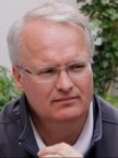 Marc
Canel, VP security systems in ARM’s SW and Systems group. Marc
Canel, VP security systems in ARM’s SW and Systems group.
Panelist
Bio: Marc Canel has extensive
experience in the mobile devices industry, driving software projects for the
past 25 years, focusing on how mobile devices work with the Enterprise
world. He is Vice President of Security Systems at ARM Inc for the past 2.5
years, leading the next generation of security architectures to become the
foundation for Enterprise applications in a connected world. He promoted the
definition of Trust systems and standards for devices in the Internet. He
defined the architecture for the next generation Root of Trust for
applications in devices. Prior to ARM Inc, he was Vice President of Software
& Security Systems at Qualcomm where he spent 18 years, focusing on the
features that make the products of Qualcomm more attractive to Enterprises.
He led Qualcomm to become a leader in the area of content protection and
privacy management. He also worked on the software ecosystem management of
Qualcomm, supporting the OEMs customers looking for complete solutions.
Prior to Qualcomm, he was at IBM for 12 years where he had various roles in
product development and management roles in data networking products.
|
|
|
|
TSI Semiconductors.
Panelist
|
 Wilbur
Catabay, SVP TDCS & Corporate Strategy, TSI Semiconductors. Wilbur
Catabay, SVP TDCS & Corporate Strategy, TSI Semiconductors.
Panelist
Bio: Wilbur Catabay is a
veteran of the semiconductor industry with more than 25 years of experience.
Recently, Mr. Catabay was VP of Technology at SVTC Technologies and prior
President of Silicon Integrated Solutions, Inc., providing Engineering
Services for Device and Process Integration. He also was Senior Director for
LSI Logic’s Foundry Engineering & Integration organization and Director of
the Advanced Process Module Development in the R&D organization. He was
responsible for evaluating and developing advanced material research for
CMOS transistors and advanced metal interconnect technology. Mr.
Catabay also worked with design and manufacturing organizations as the focal
point for implementation of new process module technology from 130nm to 45nm
CMOS technology nodes. In 1991, he was an assignee of the technical staff at
SEMATECH. Mr. Catabay has submitted more than 100 invention disclosures and
has been awarded more than 65 patents with patents pending during his tenure
with LSI Logic and SVTC Technologies. He has published more than 50
technical articles in professional journals and presented at various
technical conferences. In addition, he was the Patent Liaison and Inventor
of the year at LSI Logic and currently serves as a board member/technical
advisor for several technology firms. He attended San Jose State University
in Industrial Technology with Business Management. During his spare time,
Wilbur enjoys spending time with his family, including fishing and
photographing nature.
|
|
|
|
Mellanox Technologies
Panelist
|
 Bob
Doud – Sr. Director of Marketing – Security Technology, Mellanox Bob
Doud – Sr. Director of Marketing – Security Technology, Mellanox
Panelist
Bio: Bob brings more than 25
years experience in the networking, silicon and security industries to
Mellanox. He has previously worked at a number of networking and security
silicon companies including EZchip, Tilera, Hifn, NetOctave and SafeNet in
roles ranging from Sr. System Architect to Product Line Director. Bob also
spent a number of years in the security appliance industry in both
engineering and lead technologist roles, giving him a strong background in
the design requirements and challenges in bringing hardware & software
systems to market. Bob received a Bachelor's degree, cum laude, in Physics
and Math from Ohio Wesleyan University and holds a number of patents in the
field of communications and cryptography.
|
|
|
|
Knobbe Martens
Panelist
|
 Perry
D. Oldham, Partner, Knobbe Martens. Perry
D. Oldham, Partner, Knobbe Martens.
Panelist
Bio: Mr. Oldham represents
clients in all types of intellectual-property disputes, including those
involving patents, trademarks, trade secrets, and copyrights. His practice
is primarily focused on handling patent infringement cases. Mr. Oldham is
also registered to practice before the U.S. Patent and Trademark Office, and
has advised clients and prepared patent applications regarding a variety of
technologies. Prior to joining Knobbe Martens, Mr. Oldham designed and
supported microprocessor cores and peripherals for American Microsystems,
Inc. Mr. Oldham was awarded the Best Advocate at the Giles Rich Northeastern
Regional Moot Court held in Boston in 2001. Mr. Oldham joined the firm
in 2001 and became partner in 2007.
|
|
|
|
Intrinsic ID
Panelist
|
Dr.
Pim Tuyls, Founder and Chief Executive Officer, Intrinsic ID.
Panelist
Bio: Dr. Pim Tuyls
initiated work on Hardware Intrinsic Security™ within Philips Research in
2002. As a principal scientist, he managed the cryptography cluster in
Philips Research in which the initial research was carried out. Later he
transferred this work to Intrinsic-ID and headed the technology development.
Since 2004, Pim is a visiting professor at the COSIC institute of the
Katholieke Universiteit Leuven. His inventions have resulted in numerous
patents. He is widely accepted for his work in the security field and
Hardware Intrinsic Security in particular. Several of Pim’s papers
relating to secure implementations of Physical Unclonable Functions (PUF)
technology have been published at leading security conferences. He
co-authored the book Security with Noisy Data, which was published by
Springer in 2007.
|
|
|
|
Broadcom
|
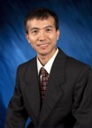 Dr.
Jerry Jiang, Senior Manager, Broadcom, IEEE Fellow. Dr.
Jerry Jiang, Senior Manager, Broadcom, IEEE Fellow.
Panelist
Bio: Dr. Xicheng Jiang
received the B.S. degree from University of Science and Technology of China,
Hefei, P. R. China and the M.S. and Ph.D. degrees in electrical engineering
from University of California, Los Angeles, CA. Since 1997, he has been with
Analog and RF microelectronics group at Broadcom, where he is a Director of
Engineering and a Broadcom Distinguished Engineer. His research interest
includes data converters, high-speed serial transceivers, cellular baseband,
Hi-Fi audio drivers, microphone interfaces and precision sensor interfaces.
Dr. Jiang is a Fellow of IEEE. He currently serves on the Technical Program
Committee of ISSCC and CICC. He is a named inventor on more than 30 issued
and pending U.S. patents and has authored or coauthored over 30 conference
and journal papers. He is the co-recipient of the CICC 2009 Best Paper Award
and the CICC 2013 Best Poster Paper Award. |
|
|
|
|
Open To Everyone
Reception & Networking
|
|
|
|
|
14th International SoC
Conference Closed.
|
|
|
|
|
|
|
|
|
* * * * * * *
* SoC Conference Program is subject to change.
Savant Company Inc, SoC Conference Organizing Committee, and Technical Advisory
Board, reserve the rights to revise or modify the SoC Conference
agenda at
its sole discretion.
Back To The Main SoC
Conference Page
|
|
Copyright © 2003-2016 by Savant Company Inc. All
Worldwide Rights Reserved. | |
|