|
| |
|
SoC Conference Presenters'
Bios & Abstracts
13h International System-on-Chip
(SoC)
Conference, Exhibit & Workshops
The Theme for This Year’s
Conference Is “Innovative SoC Solutions for Secure IoT
Applications."
|
 |
|
To present and/or exhibit at this
highly-targeted International System-on-Chip (SoC) Conference, please contact:
949-981-1837 or SoC.Conf.Update@Gmail.coma |
|
|
Click Here To
Download The UCI Campus Map
Directions &
Parking for Calit2 Building at the University of California, Irvine (UCI)
|
|
|
|
|
|
|
|
Day
One Wednesday October 21, 2015
SoC Conference Program Agenda* |
|
|
|
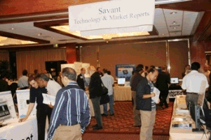
Savant
Company Inc.
 |
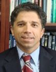
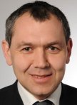
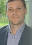
 Farhad
Mafie, SoC Conference Chairman,
IEEE OC SSCS & OCEN Chairs. Farhad
Mafie, SoC Conference Chairman,
IEEE OC SSCS & OCEN Chairs.
Welcome and Opening Remarks, Technology/Market Trends.
Farhad Mafie is SoC Conference
Chairman. He has over
20 years of experience in semiconductor and computer businesses and more
than 10 years of university-level teaching experience. He is the former Vice
President of Marketing and Engineering at Toshiba Semiconductor. He has also
worked in strategic marketing, project and design engineering at Lucent
Technologies, Unisys, and MSI Data. Farhad has a Master of Science and a
Bachelor of Science degree in Electronic Engineering from California State
University, Fullerton. He is an author and a translator, and his articles
have been published in a variety of journals and Web-based magazines on
technology and political affairs. In 2003, he published the biography of
Iranian poet and Nobel nominee who lived in exile, Nader Naderpour
(1929-2000), Iranian Poet, Thinker, Patriot. Farhad is also Editor-in-Chief
for the CRC Press SoC Design and Technologies Book Series, which includes
(1) Low-Power NoC for High-Performance SoC Design and (2) Design of
Cost-Efficient Interconnect Processing Units. Farhad is an active member of
IEEE, and he is the chair of IEEE Orange County Solid-State Circuits Society
(SSCS), as well as IEEE Orange County Entrepreneurs' Network (OCEN). He is
also a member of two UCI Advisory Committees: Communication System
Engineering and Embedded System Engineering Certificate Programs.
|
|
|
|
|
|
|
|
|
X-FAB
Semiconductor Foundries
 |
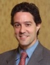
 Carlos
Stahr, Business Development, X-FAB Semiconductor Foundries. Carlos
Stahr, Business Development, X-FAB Semiconductor Foundries.
"X-FAB Process Technologies and Capabilities (Including CMOS & MEMS)."
Abstract: An introduction and overview to X-FAB process technologies and
capabilities, including CMOS & MEMS, Open Platform and Custom Process
manufacturing. This presentation will describe the different prototyping
options and typical engagement models, for engineering and production, and
finally, an overview of manufacturing facilities and points of contact will
be provided.
Bio: Carlos Stahr, Business
Development , X-FAB Semiconductor Foundries
Carlos started his career at Silicon Valley at AMD in 1983, as a circuit
design engineer, in the Microprocessors and Networking Groups, in Sunnyvale.
In 1989 he moved on to electronic design automation (EDA) and semiconductor
intellectual property (IP) where he held positions during the next 14 years
in applications and product marketing for Valid Logic, Cadence Design
Systems, COMPASS Design Automation, Virtual Chips, Phoenix Technologies and
0-In Design Automation. In 2003 he joined X-FAB Semiconductor
Foundries where he is responsible for Business Development in the Americas.
Carlos holds a BSEET Degree in Electronics Engineering Technology from
Cogswell College of San Francisco.
|
|
|
|
UCLA
 |
 Professor
Bahram Jalali, Ata Mahoubfar, Daniel Solli, Claire Chen, Cathy Jiang, Jacky
Chan. UCLA Professor
Bahram Jalali, Ata Mahoubfar, Daniel Solli, Claire Chen, Cathy Jiang, Jacky
Chan. UCLA
“Optical Computing with Silicon Photonics."
Abstract: We introduce two
types of analog optical accelerators for enhancing the performance of
electronic computing. First we discuss physical computing using complex
optical dynamics in silicon for acceleration of scientific computing. We
then present photonic computing primitives for performing nonlinear
mathematical operations.
Bio: TBA.
|
|
|
|
Broadcom

|
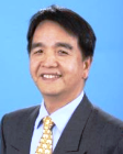
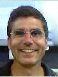
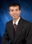 Dr.
Jerry Jiang, Senior Manager, Braoadcom, IEEE Fellow. Dr.
Jerry Jiang, Senior Manager, Braoadcom, IEEE Fellow.
“Digitally-Assisted Analog and Analog-Assisted Digital Design Techniques for
a 28 nm Mobile System-on-Chip.“
Abstract – A 28 nm 4G/LTE
mobile System-on-Chip (SoC) with digitally-assisted analog and
analog-assisted digital design techniques is presented. Multicore processors
with integrated switching regulators achieve 1.8 GHz and 1.5 GHz speeds for
A15 and A7 processors, respectively. The multiphase integrated switching
regulator achieves 90% efficiency and up to 8A current capability. PVT
monitors enable DVFS and AVS to further improve system efficiency. The
all-digital CDR achieves state-of-the-art FOMs at 0.208 mW/Gb/s and 468.75
µm2/Gb/s. An intra-bit boosting technique helps the USB2.0 TX meet the eye
mask with a 200 ps margin and reduced rise and fall times.
Bio: Dr. Xicheng Jiang
received the B.S. degree from University of Science and Technology of China,
Hefei, P. R. China and the M.S. and Ph.D. degrees in electrical engineering
from University of California, Los Angeles, CA. Since 1997, he has been with
Analog and RF microelectronics group at Broadcom, where he is a Director of
Engineering and a Broadcom Distinguished Engineer. His research interest
includes data converters, high-speed serial transceivers, cellular baseband,
Hi-Fi audio drivers, microphone interfaces and precision sensor interfaces.
Dr. Jiang is a Fellow of IEEE. He currently serves on the Technical Program
Committee of ISSCC and CICC. He is a named inventor on more than 30 issued
and pending U.S. patents and has authored or coauthored over 30 conference
and journal papers. He is the co-recipient of the CICC 2009 Best Paper Award
and the CICC 2013 Best Poster Paper Award.
|
|
|
|
Tohoku University
Japan

|
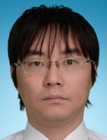 Dr.
Takeo Ohno, Associate Professor, Tohoku University, Japan. Dr.
Takeo Ohno, Associate Professor, Tohoku University, Japan.
“Nanoionic Switches for Neuromorphic Electronics.“
Abstract: In this presentation, I will talk about a new type of
electroionics-based switching memory known as an atomic switch. A solid
electrochemical reaction is used in atomic switches to control the migration
of metallic cations and their redox process in a switching operation where
an atomic-scale metal filament is formed/annihilated. Recently, several
fascinating synaptic behaviors have been demonstrated in atomic switches,
including learning ability and human memory. A switching device known as an
inorganic synapse exhibits time-dependent electrical conductance, which
enables a formation of the short-term memory and long-term memory. These
artificial synaptic behaviors maybe contribute to the construction of new
brain-type circuit.
Bio: Dr. Takeo Ohno is an Associate Professor at Tohoku University, Japan.
He received the Ph.D in materials science from Tohoku University, Japan, in
2005. From 2006 to 2007, he was a Postdoctoral Fellow at the Micro
Nanomachining Research and Education Center, Tohoku University. He was a
Postdoctoral Researcher at the National Institute for Materials Science,
Japan, from 2007 to 2012. He was also a Postdoctoral Fellow at the
University of California, Los Angeles from 2008 to 2009. His research
interests include Nanoionics Device, Neuromorphic Device and Semiconductor
Process and Device. |
|
|
|
Morning Break |
Morning Break |
|
|
|
Infineon
Technologies AG

|
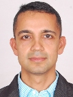 Author:
By Pankaj Singh, Principal Engineers Functional
Verification, Infineon Technologies AG. Author:
By Pankaj Singh, Principal Engineers Functional
Verification, Infineon Technologies AG.
“Comprehensive bottom up Verification Approach for Complex Automotive
Designs.“
Author:
By Martin Ruhwandl, Principal Engineers Functional
Verification, Infineon Technologies AG.
Abstract: The next generation
automotive are becoming more complex due to advanced features with 100’s of
ECU which not only control the engine but also several other electronic
system interactions. The increase in electronic component also necessitates
increased software content in car with more than 100 million lines of code
much higher when compared with facebook or F-35 fighter plan.
As the design complexity increases, the traditional way of doing
verification with HVL and other techniques such as formal verification are
not sufficient. We need different approach to ensure good quality of
verification. In this presentation we talk about using HVL like Specman for
a complete IP verification, this is also extended to next level such as bus
matrix verification with methodology to minimize the simulation run time
penalty. However as we move up to subsystem and to SoC level we take
system’s approach and adopt an advanced SystemC based methodology to look at
overall SoC verification from a holistic point of view. The
SystemC approach is also used by our customers for their system level
verification . This helps easy replication of issues and reuse of testcases
which is important to improve the verification quality apart from compliance
with traditional Specification based directed and random verification.
Besides SystemC based verification environment, we use internally developed
low level drivers for SoC verification that is commonly adopted by Virtual
prototype team, post silicon validation team and also by customers. This
further facilitates portability across different abstraction levels and
ensure a complete and consistent verification from IP , subsystem, SoC, VP,
post silicon validation.
The functionality in next Generation Automotive are quite complex with
multiple interactions across different electronic components for instance
one of the simple ADAS (Advanced Driver Assistance System) features like
Adaptive cruise control relies on sensors to check when the car ahead is
slowing down or moving into your lane, based on this information it makes an
intelligent decision to do the right thing such as applying break or moving
away to prevent collision. This requires coordination between Engine
Management Unit to interact with Electronic stability for manoeuvre and also
breaking system. Often the verification quality is not just dependent on
complexity of design but also the verification approach or verification
scenarios. We interact with concept, architecture team and customers to come
up with interesting use case scenarios for ‘Application Based Verification’
and do a complete SoC, VP and post-si validation to weed out any potential
issues before the tapeout. The hardware, software and complete VP/silicon
testing is illustrated with e-motor example for Application Based
Verification.
Bio: Pankaj completed his Bachelors in Electronics from NIT Bhopal in 1993;
Master's in Electrical Engineering from USF, Florida and an MBA from SMU,
Dallas. He has 19 years of industry experience which includes various
leadership management roles such as IP Design center Manager with GDA
Technologies, Full chip WIMAX SoC Design Manager with Texas Instruments,
Cross-site verification manager for AMD’s first ‘Heterogeneous System
Architecture’ SoC. Currently he is leading Infineon’s Automotive SoC
verification division in Singapore. He has published 21 technical
papers in various international conferences on design
implementation-verification topics such as Synthesis, DFT, Analog IP
integration, ESL and functional Verification. He has also been a board
member of few conference committees and participated in panel discussions,
invited talk.
Bio: Martin Ruhwandl studied in electronic design and information
technologies at the Technical University in Munich where he also did his
PhD. After joining Infineon Technologies AG (Communication) in 1998 he moved
to Lantiq (Wireline Communication), and went back to Infineon (Automotive)
in 2013. He is working for close to 15 years in digital functional
verification methodology and implementation, meanwhile as Principal
engineer. Besides bottom up and system verification his main area are of
work is the random based, metric driven verification. For high quality
verification with strong focus on reuse he developed and rolled out
methodologies using ‘e’ as HDL on lower level and C/SystemC on higher level
within Infineon teams. With this background he is now working on automotive
IPs and SoC platforms where these methodologies have to be further improved
and automated to hit the required safety standards (e.g. ISO 26262). The
verification methodologies has been presented in several international
conferences.
|
|
|
|
|
|
|
|
|
University of California,
Irvine
Keynote

|
 Dr.
G.P. Li, Cali2 Director, University of California, Irvine, Professor of
Engineering. Dr.
G.P. Li, Cali2 Director, University of California, Irvine, Professor of
Engineering.
Abstract: TBA.
Bio: Dr. Li is a professor at
the University of California, Irvine, with appointments in three
departments: Electrical Engineering and Computer Science, Chemical
Engineering and Materials Science, and Biomedical Engineering. At UCI, he
also serves as Calit2 division director and director of the Integrated
Nanosystems Research Facility in The Henry Samueli School of Engineering.
Dr. Li holds 18 U.S. patents, has 15 patents pending and has published more
than 280 research papers involving microelectronic technologies, microwave
circuit design, Micro-Electro-Mechanical Systems (MEMS) for communication
and biomedical instrumentation applications, and bio-nano-IT technology. He
received his bachelor’s degree in electrical engineering from National Cheng
Kung University (NCKU) in Taiwan, and his master’s and doctorate degrees,
also in electrical engineering, from UCLA. During his tenure as
a research staff member and manager of the technology group at IBM’s T. J.
Watson Research Center (1983-1988), Li worked in the area of VLSI technology
and led a research/development team to transfer the technology into the
marketplace. In 1987, he chaired a committee charged with defining IBM’s
semiconductor technology roadmap beyond the year 2000. A member of
numerous technical committees at professional conferences, Li was chair of
the Taiwan VLSI Technology, Circuit, and System Conference in 2006. He also
served as chair of the executive committee for electronics manufacturing
research and new materials at the University of California. Dr. Li received
an outstanding research contribution award from IBM (1987), two outstanding
engineering professor awards from UCI (1997 and 2001), the UCI Innovators
Award (2005), best paper award from the ITC International Telemetering
Conference (2005), and outstanding Asian American and Pacific Islander
Community Leaders and Role Models award by the Asian Business Association of
Orange County (2009). Li has been involved in several startup
companies as a co-founder or member of the technical advisory board.
Currently, he directs TechPortal, a technology business incubator housed at
the UCI division of Calit2, which supports and nurtures young companies and
university researchers commercializing their technologies. His current
research interests focus on developing technologies for efficient energy
utilization and consumption, and e-health.
|
|
|
|
Lunch |
Lunch |
|
|
|
Microsemi
Keynote

|
 Jim
Aralis, Chief Technology Officer (CTO), and Vice President of R&D, Microsemi
Corporation. Jim
Aralis, Chief Technology Officer (CTO), and Vice President of R&D, Microsemi
Corporation.
Keynote: "Down
the Technology Curve? Not so Fast"
Abstract: This
presentation will outline the new process, processor, and packaging
technologies that are enabling the expansion of mixed-signal SoC product
development efforts. Subjects that will be covered include the optimization
of design methodologies, mode partitioning, and process selection to
maximize cost-savings, performance, and time-to-market. The presenter will
also discuss how expertise in analog processing, signal conditioning,
precision timing, and high speed wired and wireless communications design
remain critical for designing differentiated products in an expanding and
evolving digital environment.
Bio: Jim Aralis has served as
chief technology officer and vice president of R&D for Microsemi since
January 2007. He has more than 30 years experience in developing custom
analog device and process technologies, analog and mixed-signal ICs and
systems, and CAD systems. Jim played a key role in transitioning Microsemi to a virtually fabless
model, supporting multiple process technologies including, high voltage and
high power BCD/CMOS, high power high integration CMOS, GaAs, SiGe, IPD, RF
CMOS SoI, GaN, SiC, and several high-density packaging technologies.
From 2000 to 2007, Jim established and served as senior design director of
Maxim Integrated Product’s engineering center in Irvine, Calif. Before that,
he spent 7 years with Texas Instruments/ Silicon Systems as mixed-signal
design head and senior principal engineer. Additional experience includes 11
years with Hughes Aircraft Company in positions of increasing responsibility
including senior scientist. Jim earned a bachelor of science degree in
Math Applied Science and Physics and a master of science in electrical
engineering from UCLA. He holds 9 patents for circuit and system design.
|
|
|
|
University
of Michigan

|
 Dr.
Mina Rais-Zadeh, Associate Professor at University of Michigan, EECS
Department. Visiting Professor, Advanced Detectors, Systems & Nanoscience,
NASA JPL. Dr.
Mina Rais-Zadeh, Associate Professor at University of Michigan, EECS
Department. Visiting Professor, Advanced Detectors, Systems & Nanoscience,
NASA JPL.
“III-Nitride on Silicon Microsystems.“
Abstract: Abstract: In the last few years we have seen rapid growth of
III-V semiconductors geared towards a variety of applications where silicon
performance falls short. GaN, a III-V semiconductor, is proven to be the
material of choice for high-frequency, high-power, and high-temperature
applications. GaN, in contrast to other commonly used piezoceramics,
exhibits piezoresistive in addition to piezoelectric effects. Although
neither the static piezoresistive nor the piezoelectric response of GaN is
particularly large, the combined piezoelectric and piezoresistive effects –
the piezoresponse – of GaN is significant. This property of GaN can be
utilized to implement a variety of microsystems on a chip having combinatory
transduction mechanisms. This talk discusses the design and few applications
of GaN microsystems in timing, integrated sensing, and acoustic
meta-materials.
Bio: Dr. Mina Rais-Zadeh received the B.S. degree in electrical engineering
from Sharif University of Technology and M.S. and Ph.D. degrees both in
Electrical and Computer Engineering from Georgia Institute of Technology in
2005 and 2008, respectively. From 2008 to 2009, she was a Postdoctoral
Research Fellow at Georgia Institute of Technology. In 2009, she joined the
University of Michigan, Ann Arbor, as an Assistant Professor of Electrical
Engineering and Computer Science (EECS). Since 2014, she has been an
Associate Professor in EECS with courtesy appointment in the Department of
Mechanical Engineering. In 2015, she is on sabbatical leave at NASA JPL. Dr.
Rais-Zadeh is the recipient of the NSF CAREER Award (2011), IEEE Electron
Device Society Early Career Award (2011), NASA Early Career Faculty Award
(2012), the Crosby Research Award from the University of Michigan (2013),
National Academy of Engineering Frontiers of Engineering (2013), ONR Young
Investigator Award (2014), and IEEE Sensors Council Early Career Technical
Achievement Award (2015). Together with her students, she received the best
poster award at the Transducers conference (2013), the best paper award at
the IEEE SiRF conference (2014), honorable mention at the IEEE IMS (2014),
and was the finalist in student paper competitions at the SiRF (2007) and
IMS (2011) conferences. She is an associate editor of IEEE Electron Device
Letters (EDL) and IEEE Journal of Microelectromechanical Systems (JMEMS) and
on editorial board of Nature Scientific Reports.
|
|
|
|
Microsemi
|
 Jim
Gallagher – Vice President of Engineering (Security Solutions), Microsemi
Corporation. Jim
Gallagher – Vice President of Engineering (Security Solutions), Microsemi
Corporation.
"Threat Driven Security."
Abstract: Threat-driven
security is a systematic system-level approach that is driven by a clear
understanding of the security need – it is not arbitrary application of
security technologies based on their perceived effectiveness or hype. Using
this systematic approach, the strength of a protection is easily gauged
through simple identification of the weakest link in the design. This
presentation will review our approach to identifying security
vulnerabilities, determining viable mitigations, and developing a threat
tree that leads to a robust threat-driven protection.
Bio: Jim joined Microsemi as
Vice President of Engineering for Security Solutions in August 2009. Jim
leads the development of software, firmware, crypto, and security products
and services to prevent reverse engineering and product tampering. Jim has
over 25 years of experience in real-time embedded software and system
development, with a strong focus on software process implementation. Prior
to joining Microsemi, Jim began his career with General Motors holding
numerous software and systems assignments. Jim holds a Bachelor of Science
degree in Electrical Engineering from the University of Notre Dame and a
Master of Software Engineering degree from Carnegie Mellon University.
|
|
|
|
Lawrence
Livermore National Laboratory
 |
 Dr.
Faranak Nekoogar, Research Staff Member Lawrence Livermore National
Laboratory Dr.
Faranak Nekoogar, Research Staff Member Lawrence Livermore National
Laboratory
"Secure Passive Tags for Hostile RF Environments"
Abstract: In many practical applications, there is an important need to use
passive (battery-free) RFID tags that operate reliably in harsh
environments. In addition, the ability to integrate various sensors such as
temperature, acceleration, acoustic, radiation, or even fiber optic seals,
to these tags are highly useful in many tagging and tracking applications.
The multiple sensor requirement increases the need for system-on-a-chip
design: while ASIC design addresses the required power budget for the
sensors and microcontrollers, the SOC techniques allows the integration of
these sub-systems. In this talk we discuss the challenges of addressing such
applications requiring secure communications and the use of multiple
sensors.
Bio: Faranak Nekoogar, Ph.D., is coauthor of "From ASICs to SOCs: A
Practical Approach," published by Prentice Hall (2003). She has worked for
many years researching UWB topics in the Department of Applied Science at
University of California, Davis. Faranak has published several patent
applications and technical papers in the following areas of UWB research:
multiple-access techniques, channel estimation, synchronization, and secure
wireless sensor networks using UWB radios. She currently conducts research
on UWB-RFIDs at Lawrence Livermore National Laboratory. She also has several
years of industry experience in functional and timing verification of
application-specific integrated circuits and systems-on-a-chip.
|
|
|
|
Microsemi
Corporation
|
 Dr.
Richard RAO, Microsemi Technical Fellow and a senior member of IEEE. Dr.
Richard RAO, Microsemi Technical Fellow and a senior member of IEEE.
“Advanced CMOS Failure Mechanisms and Design for Reliability.“
Abstract: As the IC industry
rapidly adopts new semiconductor technologies with increased density and
introduces new fabrication methods to enable novel IC structures, chip
designers wrestle with a surge of failure mechanisms. It has become
necessary to take the art of design for reliability to the next level. This
talk will give an overview of reliability failure mechanisms of an advanced
IC product focusing on the advanced Si nodes, the package and their mutual
interactions. Dr. Richard Rao will then take the audience onto a few
technical deep dives to expose some of the less well understood albeit
frequent chip failures.
Bio: Dr. Richard RAO is currently a Microsemi Technical Fellow and a senior
member of IEEE. He manages the reliability program and focuses on the
development of design for reliability (DfR) flows to deal with the
challenging reliability failure mechanisms associated with advanced
semiconductor process and packaging technology. These include the back end
and far back end interconnect Electromigration and Stress Migration;
transistor Gate Oxide Breakdown, Hot Carrier Injection and Bias Temperature
Instability; and chip to package interaction failures. He has a Ph.D. degree
in solid mechanics of materials from the University of Science and
Technology of China. Prior to joining Microsemi (Vitesse before April, 2015)
in 2004, Dr. Rao held various academic and technical positions in
reliability physics and engineering. He was an associate professor at
University of Science and Technology of China, a research fellow at
Northwestern University, USA and National Science and Technology Board of
Singapore. He also held senior and principal engineering positions in
Vitesse Semiconductor Corp, JDS Uniphase, Ericsson Inc and Motorola
Electronics. He has published over 30 papers on reliability physics and
applications and also a main contributor of several JEDEC standards. He is a
conference and session keynote speaker at International Conference on
Electronics Packaging Technology and a technical committee member for
International Reliability and Physics Symposium. He has given numerous talks
at various conferences such as IRPS (International Reliability and Physics
Symposium), ECTC (Electronics Component and Technology Conference), ISQED
(International Symposium on Quality Electronics Design), ASME Symposiums and
ICEPT, etc. Dr. Rao has over 20 years of experience and knowledge in the
advanced Si processes including 65nm and beyond nodes, flip chip and 2.5D
TSV packaging, chip to package interaction, board and system level
reliability physics and applications. He has conducted professional
development courses on advanced IC to many engineers in both IC suppliers
and users.
|
|
|
|
Panel


"FREE"
|
Panel:
“Security
Challenges in New SoC Designs: Can You Make Cents of It?"
Moderator: Farhad Mafie, SoC Conference Chairman, IEEE OC SSCS &
OCEN Chairs.
Panelists:
1. Jim Aralis, Chief Technology Officer (CTO),
and Vice President of R&D.
2. Dr. Pim
Tuyls, Founder and Chief Executive Officer, Intrinsic ID.
3. Jim Gallagher – Vice President of
Engineering (Security Solutions), Microsemi Corporation.
4. Perry D. Oldham, Partner, Knobbe Martens.
5. Dr. Per
Larsen, CEO and co-founder of Immunant, Inc.
This
Panel Is Open To Everyone . . . Register Online for FREE Panel Pass
More
Updates Coming Soon . . .
Several
Opportunities to Win various Prizes During this Panel Discussion . . .
Don't
Miss Out! |
|
|
|
Microsemi
Panelist
|
Jim
Aralis, Chief Technology Officer (CTO), and Vice President of R&D,
Microsemi Corporation.
Panelist
Bio: Jim Aralis has served as
chief technology officer and vice president of R&D for Microsemi since
January 2007. He has more than 30 years experience in developing custom
analog device and process technologies, analog and mixed-signal ICs and
systems, and CAD systems. Jim played a key role in transitioning Microsemi to a virtually fabless
model, supporting multiple process technologies including, high voltage and
high power BCD/CMOS, high power high integration CMOS, GaAs, SiGe, IPD, RF
CMOS SoI, GaN, SiC, and several high-density packaging technologies.
From 2000 to 2007, Jim established and served as senior design director of
Maxim Integrated Product’s engineering center in Irvine, Calif. Before that,
he spent 7 years with Texas Instruments/ Silicon Systems as mixed-signal
design head and senior principal engineer. Additional experience includes 11
years with Hughes Aircraft Company in positions of increasing responsibility
including senior scientist. Jim earned a bachelor of science degree in
Math Applied Science and Physics and a master of science in electrical
engineering from UCLA. He holds 9 patents for circuit and system design.
|
|
|
|
Intrinsic ID
Panelist
|
 Dr.
Pim Tuyls, Founder and Chief Executive Officer, Intrinsic ID. Dr.
Pim Tuyls, Founder and Chief Executive Officer, Intrinsic ID.
Panelist
Bio: Dr. Pim Tuyls
initiated work on Hardware Intrinsic Security™ within Philips Research in
2002. As a principal scientist, he managed the cryptography cluster in
Philips Research in which the initial research was carried out. Later he
transferred this work to Intrinsic-ID and headed the technology development.
Since 2004, Pim is a visiting professor at the COSIC institute of the
Katholieke Universiteit Leuven. His inventions have resulted in numerous
patents. He is widely accepted for his work in the security field and
Hardware Intrinsic Security in particular. Several of Pim’s papers
relating to secure implementations of Physical Unclonable Functions (PUF)
technology have been published at leading security conferences. He
co-authored the book Security with Noisy Data, which was published by
Springer in 2007.
|
|
|
|
Microsemi
Panelist
|
Jim
Gallagher – Vice President of Engineering (Security Solutions), Microsemi
Corporation.
Panelist
Bio: Jim joined Microsemi as
Vice President of Engineering for Security Solutions in August 2009. Jim
leads the development of software, firmware, crypto, and security products
and services to prevent reverse engineering and product tampering. Jim has
over 25 years of experience in real-time embedded software and system
development, with a strong focus on software process implementation. Prior
to joining Microsemi, Jim began his career with General Motors holding
numerous software and systems assignments. Jim holds a Bachelor of Science
degree in Electrical Engineering from the University of Notre Dame and a
Master of Software Engineering degree from Carnegie Mellon University.
|
|
|
|
Knobbe Martens
Panelist
|
 Perry
D. Oldham, Partner, Knobbe Martens. Perry
D. Oldham, Partner, Knobbe Martens.
Panelist
Bio: Mr. Oldham represents
clients in all types of intellectual-property disputes, including those
involving patents, trademarks, trade secrets, and copyrights. His practice
is primarily focused on handling patent infringement cases. Mr. Oldham is
also registered to practice before the U.S. Patent and Trademark Office, and
has advised clients and prepared patent applications regarding a variety of
technologies. Prior to joining Knobbe Martens, Mr. Oldham designed and
supported microprocessor cores and peripherals for American Microsystems,
Inc. Mr. Oldham was awarded the Best Advocate at the Giles Rich Northeastern
Regional Moot Court held in Boston in 2001. Mr. Oldham joined the firm
in 2001 and became partner in 2007.
|
|
|
|
Immunant, Inc.
Panelist

|
 Dr.
Per Larsen, CEO and co-founder of Immunant, Inc. Dr.
Per Larsen, CEO and co-founder of Immunant, Inc.
Panelist
Bio: Dr. Per Larsen is the CEO
and co-founder of Immunant, Inc., a spin-off from UC Irvine with a focus on
applied information security R&D. Per has co-authored numerous papers in
top-tier academic security conferences and recently authored a book on ways
to secure legacy software running atop modern hardware. In September 2015,
Per received recognition for his research contributions from the Secretary
of Defense and DARPA leadership at the DARPA Wait, What? Future Technology
Forum in St. Louis. |
|
|
|
|
Day TWO Thursday, October 22, 2015
SoC Conference Program Agenda* |
|
|
|
Savant
Company Inc.
|
Farhad
Mafie, SoC Conference Chairman,
IEEE OC SSCS & OCEN Chairs.
Bio: Farhad Mafie is SoC Conference
Chairman. He has over
20 years of experience in semiconductor and computer businesses and more
than 10 years of university-level teaching experience. He is the former Vice
President of Marketing and Engineering at Toshiba Semiconductor. He has also
worked in strategic marketing, project and design engineering at Lucent
Technologies, Unisys, and MSI Data. Farhad has a Master of Science and a
Bachelor of Science degree in Electronic Engineering from California State
University, Fullerton. He is an author and a translator, and his articles
have been published in a variety of journals and Web-based magazines on
technology and political affairs. In 2003, he published the biography of
Iranian poet and Nobel nominee who lived in exile, Nader Naderpour
(1929-2000), Iranian Poet, Thinker, Patriot. Farhad is also Editor-in-Chief
for the CRC Press SoC Design and Technologies Book Series, which includes
(1) Low-Power NoC for High-Performance SoC Design and (2) Design of
Cost-Efficient Interconnect Processing Units. Farhad is an active member of
IEEE, and he is the chair of IEEE Orange County Solid-State Circuits Society
(SSCS), as well as IEEE Orange County Entrepreneurs' Network (OCEN). He is
also a member of two UCI Advisory Committees: Communication System
Engineering and Embedded System Engineering Certificate Programs.
|
|
|
|
Indie
Semiconductor
 |
 Paul
Hollingworth, VP Sales & Marketing, Indie Semiconductor. Paul
Hollingworth, VP Sales & Marketing, Indie Semiconductor.
“Custom Microcontrollers: Using System-in-Package and Mixed Process
Technologies to Build Optimal Chips.“
Abstract: The general purpose
microcontrollers on the market today are designed to be useful across to a
broad range of applications. The reason for this is that custom design of
microcontrollers, no matter how desirable, is seen as impractical in time
and cost. indie will present a new way of building microcontrollers using
SiP - System in Package - technology, which allows NREs and timescales to be
kept low while creating parts which are optimal for the application in
question. Examples will be presented including 433MHz transceiver chips and
glucose meters; both of which use the SiP approach.
Bio: Paul Hollingworth is Vice-President of Worldwide Sales and Marketing at
indie. Prior to joining indie, he held Sales and Marketing VP-level
positions at eSilicon and Tier Logic, (a startup developing 3D FPGAs and
ASICs). Before this, he was at Altera for 13 years, running Marketing in
Europe before moving to the USA in 2004 as Senior Director of the HardCopy
ASIC Group. Paul also spent 11 years in the ASIC industry, working for LSI
Logic in England and Germany in technical and marketing roles. Paul received
a BSEE in physics and electronics and a Masters in microelectronics and
management from Durham University in England.
|
|
|
|
UC Irvine
|
 Dr.
Michael J. Klopfer, Technical Director, CalPlug - California Plug Load
Research Center, California Institute for Telecommunications and Information
Technology (Calit2), University of California, Irvine. Dr.
Michael J. Klopfer, Technical Director, CalPlug - California Plug Load
Research Center, California Institute for Telecommunications and Information
Technology (Calit2), University of California, Irvine.
"Trends in IoT Designs and
Applications."
Abstract: TBD.
Bio:
Michael is doctoral graduate in biomedical engineering. He has a background
in consumer electronics and power systems, and has designed and constructed
high-load power supplies and power management systems for x-ray generators.
He has also led numerous projects related to the planning and installation
of power, data and low voltage interface lines and assisted in the
installation and upgrade of factory automation systems.
|
|
|
|
SOITEC
 |
 George
Taylor, Sr. Manager Strategic Accounts and Business Development, Soitec. George
Taylor, Sr. Manager Strategic Accounts and Business Development, Soitec.
“SoC Architectures for the Next Generation of ULP.“
Abstract: Abstract: The FDSOI
technology with unique feature of the wide-range body bias offer
opportunities of advancing the next major step down in power consumption for
the Ultra-Low Power mobile and wearable/IoT markets. Different sections of
the SoC can be architected with different flavors of FDSOI with better
performance/power trade-offs, which enables ultra low-voltage operation
(~0.4V) and low power analog/RF SoC. In addition, FDSOI offers Dynamic
trade-off of performance vs. power for high performance, low power digital
operation.
Bio: George Taylor joined Soitec in 2014 as a Senior Manager for Business
Development. Prior to joining Soitec, George was Business Development leader
at Arteris helping strategic customers develop a new approach to SoC
architectures using the FlexNoC low power switch fabric. George has also
managed business development for SMSC/Microchip and Vitesse. Applications
Engineering and Design Consultant for Samsung and Actel/Microsemi. Field
Design and Design Engineer for ASIC devices and Library cell development at
AMI/OnSemi.
|
|
|
|
Cadence Design Systems
 |
 Frank
Schirrmeister, Senior Group Director, Product Management System &
Verification Group (SVG), Cadence Design Systems. Frank
Schirrmeister, Senior Group Director, Product Management System &
Verification Group (SVG), Cadence Design Systems.
“Navigating the Continuum of SoC Verification Engines.“
Abstract: When 100 Billion
devices connect, are networked and connected through hubs and gateways to
the cloud to enable data analytics, design diversity and complexity are
taken to new levels. As a result, new SoC architecture cycle time will be
shrinking, verification turnaround will become more aggressive and the
number of SoCs per engineer per year will increase significantly. When
choosing the most appropriate verification techniques, design teams are
facing a variety of options, spanning different levels of abstraction –
transaction-level to signal-level – and different types of execution – like
simulation, acceleration, emulation and FPGA based prototyping at the RT-level.
Exhaustive verification techniques at one level of abstraction are no longer
sufficient and need to be replaced by smart combination of
abstraction-levels and new techniques for hardware/software debug. Automated
generation of specific tests in the context of the product scenarios to be
verified require new techniques to defined scenarios involving hardware and
embedded software. This presentation will review the different verification
requirements for SoC and system development, discuss the advantages of
different hardware/software verification techniques and introduce new,
innovative solutions enabling new levels of software debug, hardware
verification and debug at the hardware/software interface. This will include
(1) multi-abstraction combinations like the Fast Models from ARM in virtual
platforms combined with hardware emulation for OS bring-up and software
driven verification in hubs and gateways, (2) Internet of Things
mixed-signal verification options in the context of embedded software for
edge node devices, (3) cycle synchronized hardware/software debug, (4)
advanced scenario definition for specific hardware/software tests at the SoC
and system-level as well as (5) re-use of verification environments between
emulation for hardware verification and FPGA based prototyping for software
development for hubs and gateways as well as server and networking devices.
Bio:
TBA.
|
|
|
|
AMD
 |
 Dr.
Juan-Antonio Carballo, Global Account Director, AMD Inc. Dr.
Juan-Antonio Carballo, Global Account Director, AMD Inc.
“Computing is the New Network. A New Golden Age for Processor SoCs,”
Abstract: When 100 Billion
devices connect, are networked and connected through hubs and gateways to
the cloud to enable data analytics, design diversity and complexity are
taken to new levels. As a result, new SoC architecture cycle time will be
shrinking, verification turnaround will become more aggressive and the
number of SoCs per engineer per year will increase significantly. When
choosing the most appropriate verification techniques, design teams are
facing a variety of options, spanning different levels of abstraction –
transaction-level to signal-level – and different types of execution – like
simulation, acceleration, emulation and FPGA based prototyping at the RT-level.
Exhaustive verification techniques at one level of abstraction are no longer
sufficient and need to be replaced by smart combination of
abstraction-levels and new techniques for hardware/software debug. Automated
generation of specific tests in the context of the product scenarios to be
verified require new techniques to defined scenarios involving hardware and
embedded software. This presentation will review the different verification
requirements for SoC and system development, discuss the advantages of
different hardware/software verification techniques and introduce new,
innovative solutions enabling new levels of software debug, hardware
verification and debug at the hardware/software interface. This will include
(1) multi-abstraction combinations like the Fast Models from ARM in virtual
platforms combined with hardware emulation for OS bring-up and software
driven verification in hubs and gateways, (2) Internet of Things
mixed-signal verification options in the context of embedded software for
edge node devices, (3) cycle synchronized hardware/software debug, (4)
advanced scenario definition for specific hardware/software tests at the SoC
and system-level as well as (5) re-use of verification environments between
emulation for hardware verification and FPGA based prototyping for software
development for hubs and gateways as well as server and networking devices.
Bio: Dr. Juan-Antonio Carballo
is AMD’s Sales Leader for the Networking and Storage Sectors globally. He is
also a successful seed-stage investor with Silicon Valley’s oldest group,
the Band of Angels. Prior to AMD, Juan-Antonio was with Broadcom Corp. where
he secured about 100 design wins with major networking and server customers
and received several Sales awards. He joined Broadcom from NetLogic
Microsystems, where he was Director of Major Accounts including the world’s
largest Wireless OEM. Prior to NetLogic, he was IBM’s Venture Capital
Executive for Semiconductors and Hardware Systems, responsible for creating
and managing strategic projects with top-tier Venture Capital firms and
their portfolio companies. Prior to this role, Juan-Antonio was leading work
in adaptive communications chips at IBM Research. He won an Division award
for his work in this area. He has filed over 30 patents and has over 20
publications in low-power design, communications systems, design economics,
and electronic design management. and wrote a widely distributed book, “Chip
Design for Non-Designers”. He is co-Chair of the International Technology
Roadmap for Semiconductors (ITRS) Design Chapters, was Chair of IEEE's DATC
Committee, and has been on the committee of many conferences. Prior
experience includes stays at Digital Equipment and LSI. Juan-Antonio holds a
Ph.D. in Electrical Engineering from the University of Michigan, an M.B.A.
from the College des Ingenieurs (Paris), and a M.Sc. in Telecommunications
Engineering from the Universidad Politecnica de Madrid. He lives in San
Francisco, sits on the board of Silicon Valley’s Spanish Association and has
run for local political office with an innovation-based platform.
|
|
|
|
Morning Break
|
Morning Break |
|
|
|
Intel
 |
 Dr.
Jeff Parkhurst, Intel Science & Technology Center Program Director Dr.
Jeff Parkhurst, Intel Science & Technology Center Program Director
Cloud Computing and Big Data.
Big Data -- Hope or Hype
Abstract: Big Data is becoming more prevalent in our daily conversation.
Mining and processing it holds the hope of providing insight into areas that
a few years ago would have been considered out of reach. Efficient
transportation for big cities, retail and genomics are all being studied
with renewed vigor. However, the promise of Big Data is also tempered by the
potential to misuse and misinterpret. This talk will look at both the
potential and the problems in working in with large amounts of data and will
take a peak into the research at the Intel Science and Technology center for
Big Data.
Bio: Dr. Jeff Parkhurst is the Program Director for three Intel Science and
Technology Centers focusing on Embedded Computing, Cloud Computing and Big
Data. He is responsible for managing the operational details in each center
as well as aiding in direction setting of the research. The Program Director
is the primary liaison between Intel and the universities on all operational
matters including contracts, IP, space, logistics, funding, and
technology/knowledge transfer. Prior to this assignment, Jeff was an
Academic Research Programs Manager working with senior technologists
internal and external to Intel setting research directions for the design
science areas of the Semiconductor Research Corporation (SRC). Jeff received
his BS from University of Nevada at Reno in 1983 and his MS from the
University of California at Davis in 1988 and his PhD at Purdue University
in 1994. Dr. Parkhurst is the author of numerous papers and one patent.
|
|
|
|
Lunch
|
Lunch |
|
|
|
Skyworks Solutions, Inc.
Keynote

|

James P. Young Vice
President, Advanced Development, Skyworks Solutions, Inc.
Keynote: "SOI RF Switch Technology & Roadmap."
Abstract: The mobile
phone has become a big part of our daily lives, which has created an
exponential growth in network data and an ever-increasing complex RF Front
End to support this growth. The RF Switch is a key component in addressing
the mobile phone RF Front End complexity by routing signals from the antenna
to various transmit and receive bands within the radio. A variety of
technologies have been used to implement the switch but today SOI is the
optimal solution. This presentation will review SOI switch requirements,
design techniques and the latest substrate technologies to address the
efficiency, linearity, size and cost requirements.
Bio: James P. Young is vice
president of advanced development at Skyworks Solutions, Inc. where he is
responsible for mobile handset power amplifier and front end module design.
His expertise includes power amplifier and RFIC circuit and system design in
CMOS, SOI, BiCMOS, bipolar, and GaAs technologies. James holds 18 patents,
has authored or co-authored over 22 papers, and taught several short courses
mainly on RFIC design. He holds a bachelor’s of science in electrical
engineering from Rose-Hulman Institute of Technology in Terra Haute,
Indiana.
|
|
|
|
IEEE Solid-State Circuits
Distinguished Lecturer, Qualcomm Technologies Inc.

|
 Dr.
Alvin Loke, IEEE Solid-State Circuits Distinguished Lecturer, Qualcomm
Technologies Inc. Dr.
Alvin Loke, IEEE Solid-State Circuits Distinguished Lecturer, Qualcomm
Technologies Inc.
"The Journey to FinFETs!"
Abstract: Despite increasing economic and technical challenges to scale
CMOS, we continue to witness unprecedented performance with fully-depleted
tri-gate devices now well in production. This tutorial seminar offers a
summary of how CMOS device technology has progressed over the past two
decades. We will review MOS device and short-channel fundamentals to
motivate how device architectures in production have evolved to incorporate
elements such as halos and spacers, mechanical strain engineering, high-K
dielectric and metal gate, fully-depleted device architectures and finally,
tri-gate finFETs.
Bio: Alvin Loke received his BASc degree from University of BC, and MS and
PhD degrees from Stanford. His doctoral work focused on copper interconnects
with low-K polymer dielectrics. From 1998 to 2001, he worked on CMOS
technology integration at HP Labs and then at Chartered Semiconductor
Manufacturing as an Agilent assignee. In 2001, he moved to Fort Collins,
Colorado where he designed CMOS PLL circuits for SerDes. From 2006 to 2013,
he was with Advanced Micro Devices where he designed high-speed
electrical/optical link circuits and addressed analog/mixed-signal concerns
for next-generation CMOS. He recently joined Qualcomm where he works on
mobile IO links. Alvin has authored over 40 publications and holds 15 US
patents. He served on the CICC technical program committee, as Guest Editor
of the IEEE Journal of Solid-State Circuits, and as an IEEE Distinguished
Lecturer. He was an active SSCS chapter officer in Fort Collins for 10
years. |
|
|
|
Panel
UC Irvine
Qualcomm
Technologies, Inc.
Atmel
Microsemi
Palmchip
"FREE"
|
Panel:
“IoT
& Wearable Applications
Driving The Next Generation of SoC Designs."
Moderator: Farhad Mafie, SoC Conference Chairman, IEEE OC SSCS &
OCEN Chairs.
Panelists:
1. Pankaj
Kedia, Sr. Director & Business Lead, Smart Wearables Segment, Qualcomm
Technologies, Inc.
2.
Dr. Juan-Antonio Carballo, Global Account
Director, AMD Inc.
3.
Jauher Zaidi, Chairman & CTO, Palmchip.
4. Dr. Michael J. Klopfer, Technical
Director, CalPlug - California Plug Load Research Center, California
Institute for Telecommunications and Information Technology (Calit2),
University of California, Irvine.
5. Mohy
Abdelgany, Engineering Vice President of Wireless Solutions at Atmel
Corporation.
6. TBA.
This
Panel Is Open To Everyone . . . Register Online for FREE Panel Pass
More
Updates Coming Soon . . .
Several
Opportunities to Win various Prizes During this Panel Discussion . . .
Don't
Miss Out! |
|
|
|
Savant Company Inc.
SoC
Conference
UCI

|
Farhad
Mafie, SoC Conference Chairman, IEEE OC SSCS & OCEN Chairs.
Moderator
Bio: Farhad Mafie is SoC
Conference Chairman. He has over 20 years of experience in semiconductor and
computer businesses and more than 10 years of university-level teaching
experience. He is the former Vice President of Marketing and Engineering at
Toshiba Semiconductor. He has also worked in strategic marketing, project
and design engineering at Lucent Technologies, Unisys, and MSI Data. Farhad
has a Master of Science and a Bachelor of Science degree in Electronic
Engineering from California State University, Fullerton. He is an author and
a translator, and his articles have been published in a variety of journals
and Web-based magazines on technology and political affairs. In 2003, he
published the biography of Iranian poet and Nobel nominee who lived in
exile, Nader Naderpour (1929-2000), Iranian Poet, Thinker, Patriot. Farhad
is also Editor-in-Chief for the CRC Press SoC Design and Technologies Book
Series, which includes (1) Low-Power NoC for High-Performance SoC Design and
(2) Design of Cost-Efficient Interconnect Processing Units. Farhad is an
active member of IEEE, and he is the chair of IEEE Orange County Solid-State
Circuits Society (SSCS), as well as IEEE Orange County Entrepreneurs'
Network (OCEN). He is also a member of two UCI Advisory Committees:
Communication System Engineering and Embedded System Engineering Certificate
Programs.
This Panel Is Open To
Everyone . . . Register for FREE Panel Pass
More
Updates Coming Soon . . .
Several Opportunities to
Win various Prizes During this Panel Discussion . . .
Don't Miss Out!
|
|
|
|
Qualcomm Technologies, Inc.
|
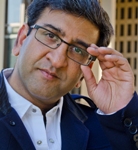 Pankaj
Kedia, Sr. Director & Business Lead, Smart Wearables Segment, Qualcomm
Technologies, Inc. Pankaj
Kedia, Sr. Director & Business Lead, Smart Wearables Segment, Qualcomm
Technologies, Inc.
Panelist.
Bio: Pankaj Kedia is Senior Director & Business Lead for the Smart Wearables
Segment at Qualcomm Technologies, Inc. In this role, Pankaj is responsible
for leading Qualcomm’s efforts to establish and grow its presence across the
wearables segments including smart eyewear, smart watches, smart bands,
smart headsets, and wearable accessories. Under Pankaj’s leadership,
Qualcomm has enabled its customers to ship 50+ products in 30+ countries
over the last year. Pankaj joined Qualcomm in late 2013 in a new business
development role and has led its efforts to incubate the wearables segment
at the company. Previously, Pankaj was the director of business
development and innovation at Intel Corporation where he was responsible for
winning, nurturing, and launching mobility products and technologies. Pankaj
launched the Intel Atom processor and led the company’s early efforts to
establish its presence and momentum in the tablet, mobile Internet device,
and smartphone categories. Earlier at Intel, Pankaj played an instrumental
role in accelerating the deployment of Notebook PCs in the industry by
defining and implementing the company’s product/marketing strategies and
launching a range of products including Centrino, Pentium 4 and Pentium III
processors. Pankaj joined Intel in 1996 and held a series of executive
advisory, strategy, marketing, planning, ecosystem, and business development
roles across the company. He holds one of the early/defining patents around
implementing low power sub-systems in mobile devices. Prior to Intel,
Pankaj was in the management consulting industry for five years leading
projects in strategy, management, and information technology. Pankaj is an
avid TED follower and has spoken at multiple TEDx events about the impact of
mobile technologies around the world. He is frequently sought after as a
speaker at industry events in the area of mobile, wearable, wireless, and
Internet, and has been extensively quoted in mainstream publications.
Pankaj holds a Master of Business Administration from Wharton, a Master of
Science from the University of Michigan, and a Bachelor of Science from the
Indian Institute of Technology.
|
|
|
|
AMD
|
Dr.
Juan-Antonio Carballo, Global Account Director, AMD Inc.
Panelist
Bio: Dr. Juan-Antonio Carballo
is AMD’s Sales Leader for the Networking and Storage Sectors globally. He is
also a successful seed-stage investor with Silicon Valley’s oldest group,
the Band of Angels. Prior to AMD, Juan-Antonio was with Broadcom Corp. where
he secured about 100 design wins with major networking and server customers
and received several Sales awards. He joined Broadcom from NetLogic
Microsystems, where he was Director of Major Accounts including the world’s
largest Wireless OEM. Prior to NetLogic, he was IBM’s Venture Capital
Executive for Semiconductors and Hardware Systems, responsible for creating
and managing strategic projects with top-tier Venture Capital firms and
their portfolio companies. Prior to this role, Juan-Antonio was leading work
in adaptive communications chips at IBM Research. He won an Division award
for his work in this area. He has filed over 30 patents and has over 20
publications in low-power design, communications systems, design economics,
and electronic design management. and wrote a widely distributed book, “Chip
Design for Non-Designers”. He is co-Chair of the International Technology
Roadmap for Semiconductors (ITRS) Design Chapters, was Chair of IEEE's DATC
Committee, and has been on the committee of many conferences. Prior
experience includes stays at Digital Equipment and LSI. Juan-Antonio holds a
Ph.D. in Electrical Engineering from the University of Michigan, an M.B.A.
from the College des Ingenieurs (Paris), and a M.Sc. in Telecommunications
Engineering from the Universidad Politecnica de Madrid. He lives in San
Francisco, sits on the board of Silicon Valley’s Spanish Association and has
run for local political office with an innovation-based platform.
|
|
|
|
Atmel
 |
 Mohy
Abdelgany, Engineering Vice President of Wireless Solutions at Atmel
Corporation. Mohy
Abdelgany, Engineering Vice President of Wireless Solutions at Atmel
Corporation.
Panelist.
Bio:
Mohy Abdelgany is the Engineering Vice President of Wireless Solutions at
Atmel Corporation, currently overseeing the development of wireless
connectivity solutions for IoT applications. Prior to joining Atmel, Mohy
was the CEO and founder of Newport Media Inc.; a fabless semiconductor
company that was acquired by Atmel in July 2014.
Mohy brings over three decades of wireless semiconductor industry experience
in engineering, marketing and GM roles. Mohy was the VP, Business Director
and Founder of RF Solutions Business Unit at Skyworks , Conexant and
Rockwell (1995-2004). Prior to joining Rockwell Semiconductor Systems, he
was a Member of Technical Staff at AT&T Bell Labs (1989-1995). He holds an
MSEE from NJIT, and a BSEE from Ain Shams University in Cairo, Egypt. Mohy
has 8 issued US Patents.
|
|
|
|
Palmchip
|
 Jauher
Zaidi, Chairman & CTO, Palmchip. Jauher
Zaidi, Chairman & CTO, Palmchip.
Panelist.
Bio:
Jauher Zaidi is Chairman & CTO of Palmchip Corporation. Jauher has over
twenty years of experience in system design and integration. Before founding
Palmchip in 1996, he was involved in system-on-chip (SoC) integration at
Quantum Corporation. Jauher received his BSEE and MSEE degrees from Pacific
States University in Los Angeles, California. He has also participated in
many SoC panels and is a recognized expert in the area of SoC development.
|
|
|
|
UC Irvine
|
Dr.
Michael J. Klopfer, Technical Director, CalPlug - California Plug Load
Research Center, California Institute for Telecommunications and Information
Technology (Calit2), University of California, Irvine.
Panelist.
Bio:
Michael is doctoral graduate in biomedical engineering. He has a background
in consumer electronics and power systems, and has designed and constructed
high-load power supplies and power management systems for x-ray generators.
He has also led numerous projects related to the planning and installation
of power, data and low voltage interface lines and assisted in the
installation and upgrade of factory automation systems.
|
|
|
|
|
Open To Everyone
Reception &
Networking
|
|
|
|
|
13th International SoC
Conference Closed.
|
|
|
|
|
|
|
|
|
* * * * * * *
* SoC Conference Program is subject to change.
Savant Company Inc, SoC Conference Organizing Committee, and Technical Advisory
Board, reserve the rights to revise or modify the SoC Conference
agenda at
its sole discretion.
Back To The Main SoC
Conference Page
|
|
Copyright © 2003-2015 by Savant Company Inc. All
Worldwide Rights Reserved. | |
|